
Countless applications require stable high frequency signal sources. Unfortunately, oscillator noise inherently increases with frequency. A frequency lock loop is a solution which has been around for many years; design techniques and analysis are well understood. The typical tradeoff is between a high frequency source that is unstable vs. a low frequency source that is very stable; and, by locking the two signal sources together, the best of both worlds can be achieved. An alternative is the use of a delay line; the circuit uses the one high frequency source, delayed in time, as its own frequency reference, eliminating the need for a second stable low frequency source. Most designs employ exclusively analog elements. An uncommon variation replaces certain analog elements with digital elements. This article outlines the design of a stable high frequency signal source utilizing a delay line approach with both analog and digital components. It also includes a brief discussion on the software required to control and linearize the circuit.
There are many approaches to frequency lock oscillator design. The circuit in Figure 1 captures the basic elements. A voltage-controlled oscillator (VCO) is driven by a control voltage, Vc. The output of the VCO is routed to an element that can “sense” a frequency variation, or drift. An element must also be included that can “compensate” for that drift. The output of the “compensate” element (the error voltage) is summed with a control voltage and fed back to the VCO in order to oppose unwanted frequency drift. The circuit in Figure 1 is a generic solution. Although there are many architectures to accomplish these functions, every solution includes these elements.
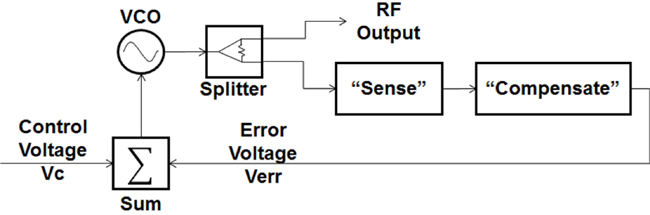
Figure 1 Simple frequency locking circuit.
THE “SENSE” ELEMENT
Mixer Basics
The “sense” element typically incorporates a mixer. A mixer is a device used to multiply two signals (see Figure 2).
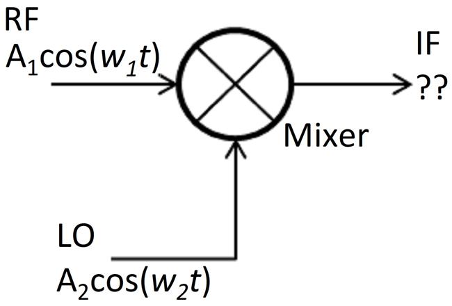
Figure 2 Basic mixer circuit.
The signal at IF is:
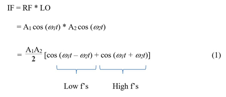
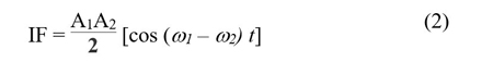
A mixer is commonly used to down convert an RF signal to a lower, intermediate frequency. Any high frequency contributions are normally filtered out, so the equation can be simplified and becomes:
Adding A Delay Line
The circuit in Figure 3 adds a delay element to the mixer circuit in Figure 2 driven by an ideal source, cos (wt).
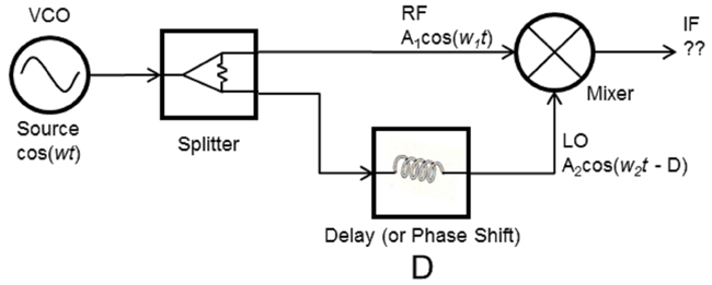
Figure 3 Adding a delay line.
The output at IF is:
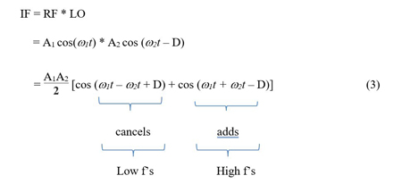
Note that the two frequencies, w1 & w2, are the same.
The resulting equation then becomes:
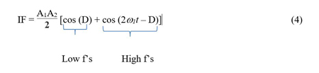
The complete design incorporates a low pass filter, so the high frequency contributions are filtered out. As such, the equation is further simplified:
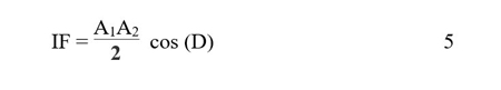
Assume the delay element, D, is a long length of semi-rigid cable (see Figure 4). A signal incident upon the delay line, which is shown as a cosine, travels down the line and eventually escapes from the other end with a phase that is clearly dependent on length L. Therefore, delay D is a function of length L and can be expressed as D(L).
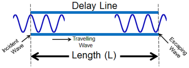
Figure 4 A wave in a delay line.
Figure 5 shows that for the same length of delay line with two distinct incident frequencies, the phase shifts are considerably different.
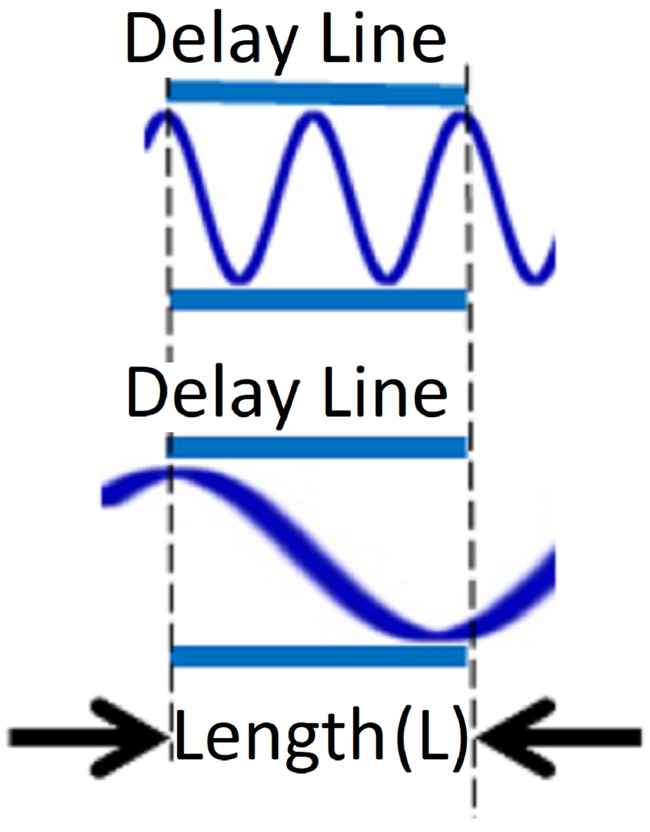
Figure 5 Two different frequencies in a length of delay line.
The delay line causes a phase shift as a function of frequency. So, D is a function of frequency and can be expressed as D(ƒ).
Equation (5) can therefore be rewritten as: