
For the circuit in Figure 16, there are two 8-bits DACs. The following questions must be answered: How many pairs of points are possible, what are those pairs and at what phase do those pairs occur? These can be answered with a simple BASIC program. The flow diagram in Figure 19 should be useful; the specific code is left to the reader. There are 1,020 combinations, the first ten of which are shown.
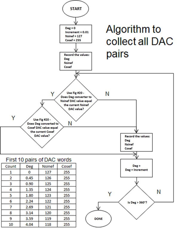
Figure 19 Algorithm to collect DAC word pairs.
PUTTING THE PIECES TOGETHER
Some new elements are introduced in the final design (see Figure 20):
- Verr is fed back to the oscillator and summed with Vc. Vc is the pre-steered voltage to put the oscillator on frequency. Verr is summed back in to correct for frequency drift. Also, a switch is added to the feedback loop to facilitate opening and closing the loop during test and linearization. Ideally, the switch is computer controlled.
- PROMs are added. As DAC words are collected, their values must be stored. External control words direct PROM look-up tables for adjusting the DACs to yield the desired frequencies. The same control word is input at three location ns simultaneously.
- A coupler is added to provide the means to access the signal.
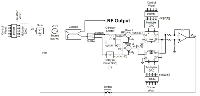
Figure 20 Completed FLL design.
Adding a Delay Line – Discussion of Length
The delay line has some physical length. In Figure 21a there is an image of a sine wave incident on a “short” length of delay line. In this case, the delay line is one wavelength long. Clearly, as the sine wave escapes from the delay line its phase is 0 degrees, i.e. there is zero phase shift.
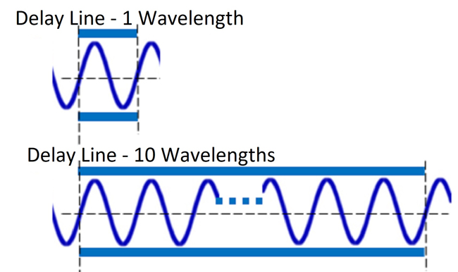
Figure 21 Delay line length: 1 wavelength (a) and ten wavelengths (b).
If the frequency of the wave increases, its wavelength becomes shorter and the phase of the escaping wave becomes a value greater than zero. For example, the frequency could increase by some amount such that the escaping wave now has 1 degree of positive phase shift. If this were the case, to be useful the detection circuit must be sensitive enough to measure the 1 degree phase shift in order to compensate for it.
If, however, the delay line were ten times longer, i.e. ten wavelengths long (see Figure 21b), the 1 degree of phase shift per wavelength is additive. In other words, the escaping wave will now be shifted by 10 degrees.
As the length of delay line increases, the sensitivity of the loop increases. For locking a loop, this is referred to as the capture window. As the frequency shifts slightly, there is a band of frequencies, or capture window, within which the loop is able to sense and correct for frequency error.
Adding a Delay Line – Discussion of Temperature Stability.
A nice property of a delay line formed from semi-rigid cable is its temperature stability. Because the length of line is important, any change will negatively impact circuit performance. Semi-rigid cable is inherently rugged with regard to environmental conditions, so for most use cases the effect of temperature on electrical length is an insignificant source for error. In extreme environments, however, a thermoelectric heater is sometimes used.
LINEARIZATION
The VCO will not tune linearly without pairing and calibration with the DAC. During linearization, the VCO is swept through its range by the DAC and the resulting frequencies are measured. Because delay lines behave differently at different frequencies, the delay line DACs are also swept through their range. During linearization, the circuit is characterized and digital words are collected. Those digital words are then stored in PROM look-up tables. The calibration steps are summarized below:
- During linearization, the switch in the feedback loop must be open. Otherwise the loop will try to acquire, it will push the oscillator, and the data collected will be erroneous.
- With the circuit running open loop, increment the Vc DAC until the desired frequency is reached. This DAC value will be the first pre-steered value.
- Measure Verr. Of course, it is desired to have Verr to be zero.
- While monitoring Verr, begin sweeping through the cos/-sin DAC values using the using the 1,020 pairs of possible words.
- Continue through these pairs of words until Verr is as close to zero as possible. Since it is sweeping sinusoidally, it will approach zero and begin moving away, so dither it until the best Verr is determined.
- The circuit may be operating at the wrong locking point, as illustrated in Figure 7. It is straightforward to check by simply closing the loop. If the oscillator stays at the proper frequency, then it is at the correct point on the curve. If, however, it tunes off the desired frequency, then the Verr DAC value is incorrect.
- If the Verr DAC value is incorrect, then open the loop and continue sweeping through the set of cos/-sin DAC values until Verr returns to zero with another pair of words.
- Once again check to see if the set of words is correct by closing the loop.
- Once the proper point on the linearization curve is determined, repeat the process through all Vc DAC values required for proper operation. Once the correct point on the curve is found, all subsequent DAC words will be relatively close.
- After all data is collected, program the PROMs.
SUMMARY
A solution to the problem of stabilizing an inherently noisy high frequency oscillator using a delay line employs both analog and digital elements and includes a brief discussion on the software required to control and linearize the final circuit. An advantage of the delay line approach over more common frequency and phase lock loop solutions is the absence of a separate LO. This solution presumes the VCO has some minimum level of stability and then uses itself, delayed in time, as its own reference source. If frequency errors occur, it “senses” and compensates for its own drift. Delay lines realized with semi-rigid cable are relatively stable in most cases and can be environmentally stabilized if necessary. A significant variation is the use of digital elements in place of their more common analog counterparts. The digital elements have less variability, are more standardized and are more cost effective than their analog counterparts.
Biographies
Danny Polidi received his B.S. and M.S. degrees in Electrical Engineering from the California Polytechnic State University, San Luis Obispo, CA in 1990 and 1991. He is currently a PhD candidate in Systems Engineering at CSU. Upon graduation, he started working at Space Systems/Loral on high frequency, microwave designs for space applications. Later, at Radian Technology, he became product manager of the Digitally Tuned Oscillator Product Line where he was responsible for designing new circuits, writing code and production support. At NANOmetrics, Danny managed all electronic engineering activities. From 2004 to present he has worked at Raytheon as a section manager, team lead and cost account manager.
Mike Crist received his B.S. in Computer Science from Embry-Riddle Aeronautical University in 2003 and his M.S. in Electrical Engineering from The University of Texas at Dallas in 2005. He is currently enrolled at Colorado State University working on a PhD in systems engineering. Mike has had a variety of roles over his 20+ year career, including embedded software developer, FPGA developer, circuit card designer, cost account manager, integrated product team lead and engineering tool strategist. He currently works on staff for an Electrical / Mechanical Design Center on various model-based engineering projects.