
The significance of the quadrature outputs is that all the variables and unknowns are eliminated. Consider points A & B in Figure 11. The correct location in time is indistinguishable by viewing the voltage of the cosine curve, alone; however, if the voltage along the sin curve is simultaneously monitored, the ambiguity is resolved. For example, if the cosine decreases in voltage and the sin decreases in voltage, then the circuit could only be at location B and moving to the left. There is now a means to sense and quantify the source oscillator frequency drift.
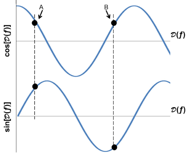
Figure 11 Simplified representation of Figure 9.
THE “COMPENSATION” ELEMENT
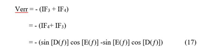
The purpose of this circuit (see Figure 12) is to translate frequency drift information into a useful error voltage. For this, the output voltage Verr is calculated.
E is a function of frequency and is arbitrarily defined such that:

The signal at node IF3 is:

Similarly, the signal at node IF4 is:

Verr is then:
Which simplifies to:

Equation (18) when compared with the Equation (14) implies that Verr is equal to zero for all frequencies ƒ. It has thus been derived that Verr is conditionally equal to zero for all frequencies ƒ if Equation (14) is true and E(ƒ) is controlled. E(ƒ) is constructed so that Equation (14) is true and, therefore, Verr = 0.
To tune the VCO (see Figure 1), a control voltage (Vc) is applied. As Vc changes, the VCO frequency should correspondingly change in a predictable and repeatable fashion. If it does not, a resulting error voltage (Verr) is added to correct any deviation. When the VCO frequency returns to its desired value, Verr returns to zero. This all depends upon the function E(ƒ).
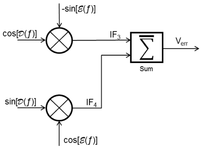
Figure 12 Compensation circuit.
The circuit in Figure 12 uses two mixers. As discussed earlier, a mixer is used to multiply two signals. The discussion to this point has been strictly about analog electronics, which been used successfully for many years. However, in the next section, some analog components are replaced with digital components.
The Multiplier
The circuit in Figure 12 is illustrated solely with analog components. There exist available digital counterparts as shown in Figure 13, where a multiplier integrated circuit (IC) and a digital-to-analog converter (DAC) replace the analog mixer. The two signals to be multiplied are applied to Ports X and Y. At Port X, the familiar signal cos [D(ƒ)] appears. The signal at Port Y is supplied by the DAC.
Figure 13 Digital multiplier IC and DAC.
Controlling the DAC
A DAC is a device that takes a digital word and converts it to an analog voltage. In this case, an 8-bit DAC is used. With 8-bits per word, there are 28 = 256 words, where the range is 0 to 255. A sample of DAC output voltages is shown in Figure 14.
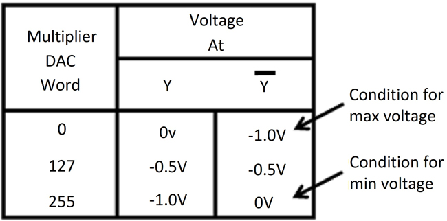
Figure 14 DAC input words and output voltages.
If it is desired to produce a sinusoidal signal at Y, then it is only necessary to increment the 8-Bit multiplier DAC digital word between 0 and 255 at a sinusoidal rate (see Figure 15). The analog circuit in Figure 12 can now be realized with the hybrid approach in Figure 16.
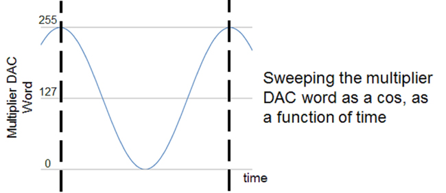
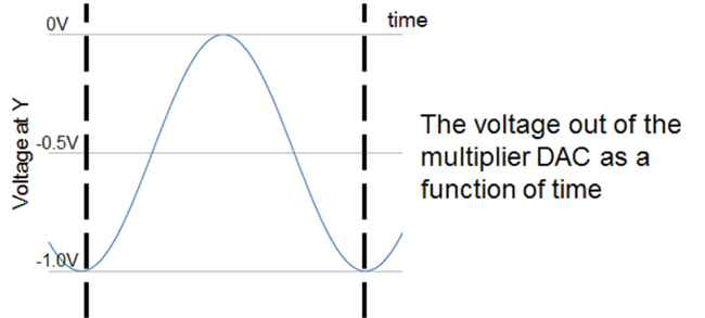
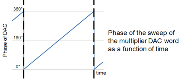
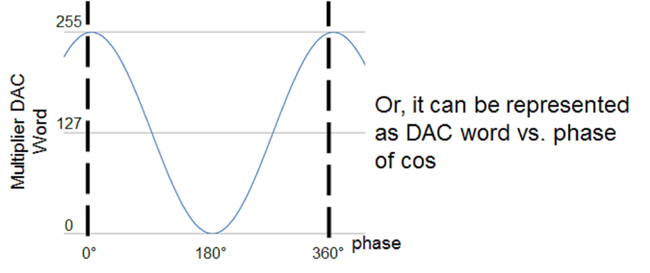
Figure 15 DAC digital input versus time (a), analog output voltage versus time (b), output phase versus time (c) and DAC digital input word versus phase (c).
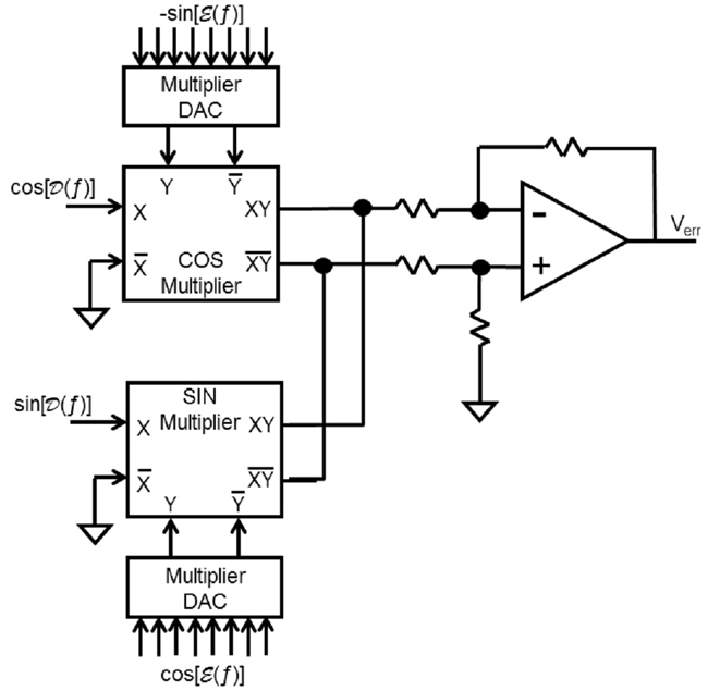
Figure 16 Realized compensation circuit.
The pair of curves in Figure 17 represent the curves for the cos [E(ƒ)] and – sin [E(ƒ)] functions. If a vertical line were drawn through the curves in Figure 17, it would intersect the curves at a pair of points. Figure 18, for example, captures a few obvious pairs.
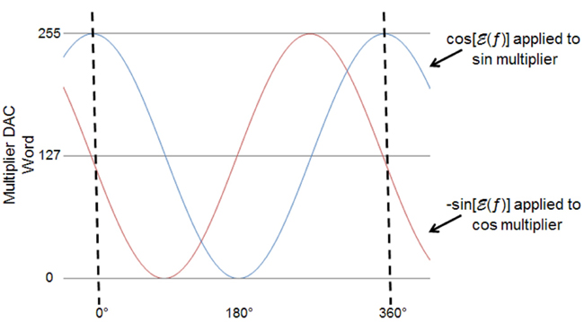
Figure 17 Multiplier DAC word vs phase.
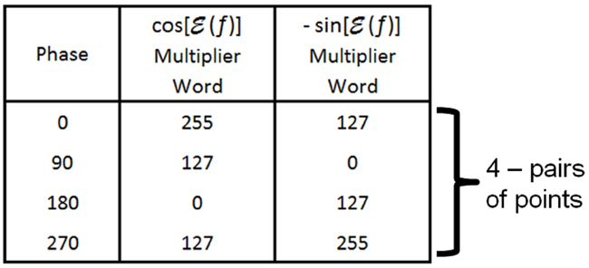
Figure 18 Several DAC word pairs.