

This article presents a compact 4×4 active antenna array (AA) operating in the 27 to 29.75 GHz 5G frequency range 2 (FR2) band. The array employs four identical 2×2 antenna-in-package subarray modules (SaMs) and a custom 16-way beamforming network (BFN) integrated into a multilayer printed circuit board (PCB). A high linearity power amplifier (PA) module provides the transmit gain. Full-wave simulations in CST Studio Suite were used to optimize the feed network and predict S-parameters, radiation patterns and effective isotropic radiated power (EIRP). A prototype was fabricated and measured in an anechoic chamber. The active array achieves a boresight EIRP of about +40.7 dBm at 28.375 GHz with a half-power beamwidth of approximately 25 degrees in both planes, sidelobe levels below -12 dB and cross-polarization discrimination exceeding 25 dB. These results satisfy the demanding requirements for 5G base station antennas and demonstrate that a modular approach can deliver high gain while retaining compactness. The design also lends itself to scalable phased arrays; future work will extend the architecture to beam-steerable, dual polarized and wider-band systems.
Millimeter-wave frequencies are central to 5G and beyond wireless networks because they provide large available bandwidths. However, the associated free-space path loss and atmospheric attenuation require transmitters with high gain and EIRP. Active AAs at these frequencies offer advantages over passive arrays. They integrate power amplification, beamforming and radiating functions, reducing losses and enabling compact front-ends. This work focuses on the design and characterization of a 4×4 planar active array tailored to the 27 to 29.75 GHz segment of the FR2 band, encompassing portions of 3GPP bands n257 and n258, as well as the entire band n261. The design aims to radiate a broadside beam with single linear polarization and an EIRP exceeding +39 dBm across the band, while maintaining cross-polarization discrimination above 25 dB and a half-power beamwidth (HPBW) of 25 degrees in both the E- and H-planes. Achieving these goals in a wideband mmWave architecture requires careful co-design of radiating elements, feed network and active circuitry.
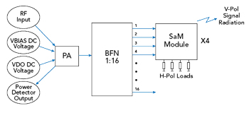
Figure 1 Functional block diagram of the proposed 4×4 active AA. This layout highlights how the PA feeds the BFN, which splits the signal to excite the four SaMs on the top layer.
Beyond the simple requirement of high gain, modern base station antennas must also maintain consistent performance across the entire operating band and environmental conditions. mmWave arrays often exhibit beam squint — the steering of the main lobe when frequency changes — because of fixed feed network delays. They are also susceptible to mutual coupling between elements, which can raise sidelobe levels or introduce beam-shaping errors. Therefore, the proposed array (see Figure 1) is designed with balanced line lengths and mirror-symmetric excitation to mitigate these issues. Additionally, because the array will be driven by a single PA, the feed network must distribute equal power to all radiating ports while introducing specific phase differences among them. This arrangement ensures the fields from each element combine coherently along the array normal, maximizing gain and enhancing polarization purity.
To meet the gain and beamwidth requirements, we adopt a 4×4 rectangular lattice. Sixteen radiating elements provide an extra array gain of approximately 12 dB relative to a single radiating element, assuming uniform illumination. A modular approach1 simplifies assembly and enables scaling. Four identical 2×2 antenna modules2 serve as the building blocks of the aperture. Each module houses four dual polarized dielectric-filled cavity antennas implemented on a low-temperature co-fired ceramic (LTCC) substrate.3-8 Only one polarization is excited in this prototype, and the unused ports are terminated on the PCB, effectively creating a single-polarized 4×4 aperture. A corporate beamforming network splits the PA output into 16 equal amplitude, in-phase signals; relative phase shifts of 180 degrees are introduced where needed to enforce a mirror-symmetric excitation within each module. This sequential rotation feeding9 improves pattern symmetry and suppresses cross-polarization. A high linearity GaAs pHEMT PA provides sufficient gain and linearity to meet the EIRP target and support high-order modulation schemes. The entire assembly is integrated into a five-layer PCB, with the SaMs on the top side, the BFN buried in an inner layer and the PA mounted on the bottom side.
SAM DESIGN AND ARRAY CONFIGURATION
The individual SaM (see Figure 2) measures 10 × 10 × 1.5 mm and integrates a 2×2 subarray of dielectric-filled cavity antennas. The alumina-glass composite LTCC package (εr ≈ 6.6, tanδ ≈ 0.007) offers stable RF performance and efficient thermal management. Each element supports two orthogonal polarizations via aperture-coupled striplines. Each dielectric cavity resonator operates in the TE11 mode and is loaded with a metasurface on the top layer to control the radiation pattern and impedance bandwidth. The coaxial feed pins, arranged in a ball grid array (BGA), facilitate easy integration onto the host PCB. The inter-element spacing within the module is about 5 mm (≈ 0.47λ0 at 28 GHz), close to half a wavelength to mitigate mutual coupling and avoid grating lobes. The module’s feed network uses a mirror-symmetric configuration, as seen in Figure 3).9 When the four elements are driven with equal-magnitude signals, diametrically opposite elements receive a 180-degree phase shift relative to one another. This sequential rotation excites the elements such that their co-polar fields add coherently along boresight while cross-polar components cancel, yielding cross-polarization discrimination of more than 25 dB. The unused polarization ports are equipped with 50 Ω loads to ensure proper termination and prevent unwanted resonances.
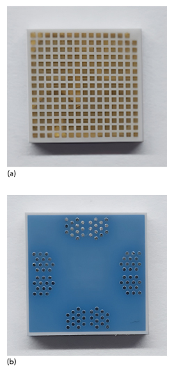
Figure 2 Top (a) and bottom (b) views of an individual 2×2 antenna-in-package (SaM) module used in the array.
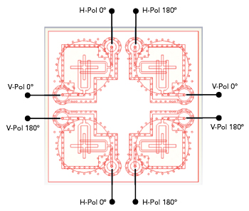
Figure 3 Pin configuration of the 2×2 SaM, indicating the required phasing of inputs for in-phase excitation of the four radiating elements in both H- and V-polarization ports.
Four SaMs are arranged in a 2×2 grid on the top layer of the host PCB, forming the 4×4 array aperture. A small gap (≈ 0.4 mm) between modules accommodates manufacturing tolerances. The resulting element spacing between adjacent modules is about 0.51λ0 at 28 GHz — sufficient to avoid grating lobes across the 27 to 29.75 GHz band. A ring of electromagnetic bandgap (EBG) “mushroom” structures surrounds the modules to suppress surface waves on the PCB and preserve a well-behaved radiation pattern. These mushroom cells consist of metal patches connected to the lower ground plane by vias, creating a high-impedance surface that minimizes surface-wave propagation. The overall board size is about 58 × 58 mm, which accommodates the four modules, feed network routing and active circuits while leaving space at the periphery for mounting hardware. The modular concept means larger arrays can be realized simply by tiling more SaMs and replicating the corresponding feed network sections.
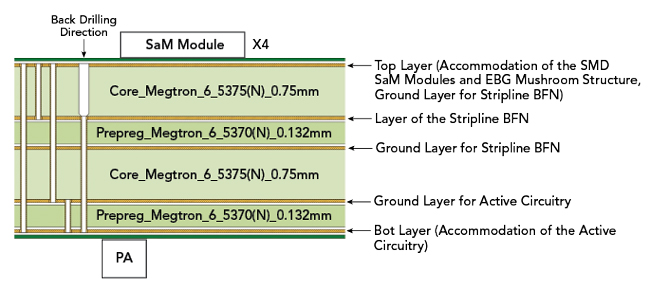
Figure 4 Cross-sectional stack-up of the host PCB, showing the multi-layer structure (core and prepreg layers) and their thicknesses.
PCB ARCHITECTURE AND BEAMFORMING NETWORK
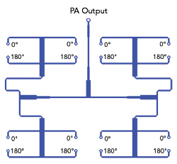
Figure 5 Top-view layout of the 16-way stripline beamforming network (BFN) integrated in the host PCB.
The host PCB (see Figure 4) is fabricated on a Panasonic Megtron 6 laminate with five copper layers. The top layer provides mechanical and RF interfaces for the SaMs and includes the EBG structures. The second layer implements the beamforming network. This corporate feed divides the PA output into 16 equal signals, four for each module and introduces 180-degree phase shifts where required by using half-wavelength line extensions at the design center frequency. The stripline BFN (see Figure 5) is routed between ground planes on Layers 1 and 3 to achieve a homogeneous dielectric environment and minimize losses. Layers 3 and 4 primarily serve as ground and shielding planes. The fifth (bottom) layer hosts the PA and other surface-mount devices. Blind vias 1:2 connect the BFN outputs to the SaM feed pins, while a blind via 2:5 brings the PA output up to the BFN input. The unused polarization ports are connected through vias to on-board 50 Ω terminations on the bottom layer.