

Careful inter-layer routing is essential at mmWave frequencies. The PA output is connected to the BFN through a blind via 2:5, which is back-drilled from the top to remove stub lengths and reduce parasitic inductance. Each of the 16 BFN outputs is delivered to a SaM feed through a blind via 1:2, minimizing transition losses. Conversely, the 16 unused polarization ports are fed by through vias to the bottom layer; because these paths carry RF power to the 50 Ω terminations, their slightly higher parasitic inductance does not degrade performance. The entire BFN on Layer 2 is surrounded by a fence of plated vias 1:4, forming a vertical “cage” that prevents the propagation of parallel-plate modes between the neighboring ground planes. This ensures that the feed network performance is insensitive to board dimensions and suppresses coupling between adjacent BFN lines.
Full-wave simulations guided the BFN design. Initial circuit calculations ensured proper impedance matching at each power splitter junction. 3D electromagnetic models of the junctions, delay lines and via transitions were then optimized using CST’s frequency-domain solver. Finally, the entire feed network with SaM models was simulated using the time-domain solver. The resulting S-parameters show return losses better than 12 dB across 27 to 29.75 GHz and amplitude imbalance within 0.5 dB across all 16 outputs. The relative phases at the outputs closely match the required 0-degree/180-degree configuration, enabling coherent excitation of the aperture. Simulated array patterns indicate a broadside beam with HPBW of about 25 degrees in both principal planes and cross-polarization levels 25 dB below the co-polar maximum. A minor beam squint of a few degrees at the band edges is observed because the fixed λ0/2 delay lines yield slightly different phase shifts away from the center frequency.
PA AND ACTIVE CIRCUITRY
The active array employs a single high linearity PA to drive all 16 antenna ports. The chosen device, Altum RF’s ARF1026Q4, is a GaAs pHEMT amplifier optimized for 27 to 31.5 GHz operation and packaged in a 4 × 4 mm QFN. It provides approximately 28 dB small-signal gain with ±1 dB flatness (see Figure 6) and can deliver about +26 dBm output at 1 dB compression (P1dB) (see Figure 7), with a saturated output of roughly 29 to 30 dBm. Its third-order output intercept point (OIP3) is around +36 dBm, ensuring good linearity for wideband modulated signals. The device exhibits input and output return losses better than 10 dB across the band, easing integration into the feed network. High linearity ensures the PA can handle signals with high peak-to-average power ratios, such as 256-QAM, without introducing significant spectral regrowth.
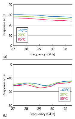
Figure 6 Measured small-signal gain (a) and input return loss (b) of the power amplifier vs. temperature. The PA provides approximately 28 dB gain with less than ±1 dB variation across the tested temperature range.
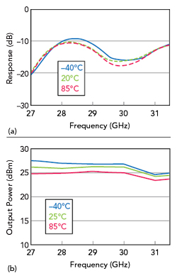
Figure 7 Measured output return loss (a) and output 1 dB compression point (b) of the PA vs. temperature. The output port maintains better than 10 dB return loss across the band at all temperatures.
The PA’s integrated bias circuitry is powered from a 4 V supply and draws approximately 600 mA. In our implementation, separate connectors provide the drain supply and gate control, enabling bias adjustment during testing. Bypass capacitors at the package leads suppress RF leakage into the supply network. A built-in power detector delivers a DC voltage proportional to the RF output, which is routed to a DC connector on the board for monitoring output power. Such detectors are useful for calibration and adaptive power control in real-world deployments.
The PA is mounted on the bottom layer of the PCB, with its output coupled to the BFN via a plated-through hole and its input fed via a coaxial connector. Proper thermal management is critical: the PA sits on a metallized thermal pad with multiple vias to spread heat into the ground planes, and the LTCC modules also aid thermal dissipation because of their high thermal conductivity and exposed metal surfaces. The array’s total DC power consumption at the PA’s P1dB is about 2.7 W. Nevertheless, because only a single PA is used to drive the entire array, the overall transmitter efficiency is limited by the losses of the passive feed network and subarray modules. Future designs may incorporate distributed amplification or multiple gain stages — one per module or per row — to further improve efficiency and EIRP.
SIMULATION RESULTS
Extensive electromagnetic simulations were performed to predict the array’s behavior. Combining the BFN with the SaM embedded element patterns yields a realized antenna gain of roughly 14 dBi at 28.375 GHz and slightly lower gains at the band edges. When driven with the PA delivering +26 dBm at its output, the resulting EIRP is about +40 dBm at the center frequency and remains above +39 dBm across 27 to 29.75 GHz. The simulated radiation patterns exhibit HPBWs of approximately 25 degrees in both the E- and H-planes, with peak sidelobe levels near -12 dB. Cross-polarization discrimination exceeds 25 dB across the operating band, thanks to the sequential rotation feeding scheme. The amplitude imbalance across the 16 ports at the band edges remains within 0.5 dB, and the phase error is within ±8 degrees of the design target. Minor beam tilting at the band edges is predicted due to the frequency-dependent phase errors from the fixed delay lines; however, the main beam remains within a few degrees of boresight over the entire operating band. These results confirm that the integrated design meets the targeted gain, radiation pattern and polarization purity requirements.
The transmitter efficiency was also estimated from simulation data. Based on a power-added efficiency of 15 percent for the PA at its 1 dB compression point and a total efficiency of 55 percent for the AA, the overall system efficiency is found to be approximately 8.3 percent, with a DC power consumption of around 2.7 W, which aligns well with the measured results. The simulation also predicts a robust input match at the PA port, with input return loss better than 12 dB across the band, ensuring minimal reflected power back to the driver.
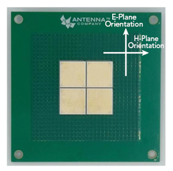
Figure 8 Photograph of the fabricated 4×4 active antenna array prototype – top side (radiating aperture). The four integrated SaMs are visible as square patches in the center of the green PCB, and a ring of mushroom-type EBG via holes surrounds them to suppress surface waves.
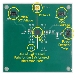
Figure 9 Photograph of the fabricated 4×4 AA prototype – bottom side (active circuit). This view shows the PA mounted at the center of the PCB backside, along with its biasing network. The RF input connector (top center mini-SMP) and two DC supply connectors are installed on this side.
FABRICATED PROTOTYPE AND MEASUREMENTS
A prototype of the 4×4 active AA (see Figures 8 and 9) was fabricated to validate the design experimentally. The five-layer PCB used precision laser-drilled microvias and the SaMs were integrated using a reflow process. The PA and other surface-mount components related to the active circuitry were assembled on the bottom side. A spherical far-field anechoic chamber was employed to measure the radiation characteristics (see Figure 10). The array was mounted on a fixture to record both co-polar and cross-polar patterns in the E- and H-planes over the frequency range 27 to 29.75 GHz. During pattern measurements, the PA was driven well below compression to avoid nonlinear distortion. A reference horn antenna with known gain was used to calibrate the measurement setup, and polarization discrimination was measured by rotating the receiving horn orthogonally. EIRP measurements were conducted by increasing the input power until the PA reached its 1 dB compression point.
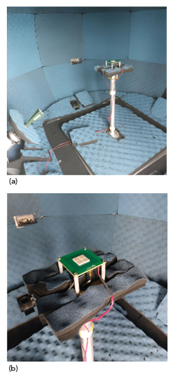
Figure 10 Photographs of the antenna array prototype undergoing EIRP (far-field power) measurements in a spherical anechoic chamber. Wide-angle view of the measurement setup (a) and close-up view (b).
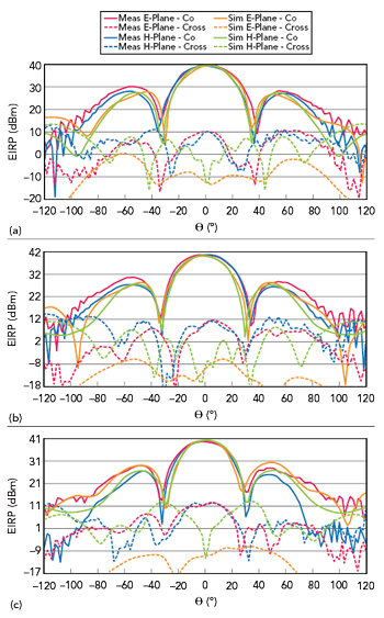
Figure 11 Measured and simulated co-polar and cross-polar far-field radiation patterns of the 4×4 array in both the E-plane and H-plane at 27 GHz (a), 28.375 GHz (b) and 29.75 GHz (c).
The measured radiation patterns agree closely with simulations (see Figure 11). At 28.375 GHz, the array produces a broadside beam with an HPBW of about 25 degrees in both principal planes, with sidelobes suppressed by roughly 12 dB. Cross-polarization levels are at least 25 dB below the co-polar main lobe at boresight and remain more than 20 dB down over the HPBW. At 27 GHz and 29.75 GHz, the beam shape remains similar; a slight beam squint of 1 to 2 degrees is observed, consistent with simulations. When the PA is driven to P1dB, the array radiates approximately +40.7 dBm EIRP at 28.375 GHz and over +39 dBm at the band edges. Using the PA output power estimated from the measured DC voltage and the measured EIRP value, the realized gain of the AA at the center frequency is found to be 14 dBi. The DC power draw during these measurements is about 2.7 W, while the dissipated power is 2.5 W, yielding an overall efficiency of about 8 percent. The input reflection coefficient at the PA port is better than 12 dB across the band, indicating proper matching and stable operation. The array shows no evidence of oscillations or spurious radiation, validating the bias and decoupling design.
CONCLUSION
This work has presented the design, simulation and experimental validation of a compact 4×4 active AA for the 27 to 29.75 GHz 5G FR2 band. Four identical SaMs based on LTCC technology provide the radiating aperture, while an embedded stripline beamforming network ensures equal amplitude and appropriate phase distribution for coherent broadside radiation. A high linearity GaAs PA drives the array, delivering a combined EIRP of around +40 dBm. The modular approach simplifies assembly and allows the array to be scaled by tiling additional modules, offering a path toward larger phased arrays. Simulations and measurements demonstrate that the array meets requirements for gain, beamwidth, sidelobe suppression and polarization purity. Minor beam squint at the band edges has been observed; future work will explore feed networks with broadband phase compensation to flatten the phase response. Extending the design to dual polarized and beam-steerable configurations is another goal, as is improving the RF efficiency through distributed amplification or integration of multiple PA stages. The techniques demonstrated here — such as sequential rotation feeding, integrated BFN design and modular assembly — are broadly applicable to mmWave transceivers and lay a foundation for scalable, high performance AAs for 5G and beyond.
References
- B. Sadhu, X. Gu and A. Valdes-Garcia, “The More (Antennas), The Merrier: A Survey of Silicon-Based mm-Wave Phased Arrays Using Multi-IC Scaling,” IEEE Microw. Mag., Vol. 20, No. 12, 2019, pp. 32–50.
- Y. Zhang, S. Ogurtsov, V. Vasilev, A. Vilenskiy, A. A. Kishk, M. V. Ivashina and D. Caratelli, “Dual-Polarized Dielectric-Filled Cavity Antenna with Air-Gap-Free Metasurface Loading for LTCC-Based 5G-and-Beyond Antenna-in-Package Phased Arrays,” IEEE Trans. Antennas Propag., Vol. 74, No. 2, Feb. 2026, pp. 1293-1307, doi: 10.1109/TAP.2025.3634999.
- D. G. Kam, D. Liu, A. Natarajan, S. Reynolds, H.-C. Chen and B. A. Floyd, “LTCC Packages with Embedded Phased-Array Antennas for 60 GHz Communications,” IEEE Microw. Wirel. Compon. Lett., Vol. 21, No. 3, 2011, pp. 142–144.
- C. Zhou, W. Yang, Q. Xue, Y. Liu, Y. Xu and W. Che, “Millimeter-Wave Wideband Dual-Polarized LTCC Antenna Array Based on Metasurfaces for Beam-Scanning Applications,” IEEE Trans. Antennas Propag., Vol. 70, No. 10, 2022, pp. 9912–9917.
- D. Chen, W. Yang, S. Pan, Q. Xue and W. Che, “Millimeter-Wave 45°-Polarized LTCC Phased Array Using Wide-Beam Patch–Via-Wall Elements for Wide-Angle Scanning Applications,” IEEE Trans. Antennas Propag., Vol. 71, No. 12, 2023, pp. 9497–9508.
- M. Alhenawy and M. Schneider, “Antenna-in-Package (AiP) in mm-Wave Band,” Int. J. Microw. Wirel. Technol., Vol. 5, No. 1, 2013, pp. 55–64.
- G. Theis, Z. Song, G. Federico, D. Caratelli and A. B. Smolders, “A Design Framework for Beamforming Integrated Circuits Operating at mm-wave Frequencies,” IEEE Access, Vol. 9, 2021, pp. 62232–62240.
- Y. Zhang, S. Ogurtsov, V. Vasilev and D. Caratelli, “2D Beam-Steerable Array Antennas for 5G Antenna-in-Package Applications,” Proc. IEEE International Workshop on Antenna Technology (iWAT), 2024, pp. 75–77.
- J. Granholm and K. Woelders, “Dual Polarization Stacked Microstrip Patch Antenna Array with Very Low Cross-Polarization,” IEEE Trans. Antennas Propag., Vol. 49, No. 10, Oct. 2001, pp. 1393–1402.