
After serving as something of a cash cow for HP and then Agilent Technologies, the electronic measurement business is now charting its own course as an independent company – Keysight Technologies. Microwave Journal was honored to be the first of the industry trade media to visit and tour Keysight’s new Santa Rosa headquarters. This special report summarizes what we saw and learned.
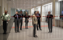
Figure 1 Wall listing all Hewlett Packard – Agilent – Keysight Technologies' patents since 1939.
Reborn. As they rang the bell at the New York Stock exchange on November 3, Keysight Technologies returned to its roots in electronic measurement, the last step in splitting off from Agilent Technologies to become a separate company. Grown out of Bill Hewlett’s and Dave Packard’s audio oscillator, invented in the famous garage in Palo Alto in 1939, HP became so large that it split in 1999, with the electronics group becoming Agilent Technologies. Agilent grew its two businesses in electronic measurement and life sciences into dominant segments in their respective markets. Yet each was different. With time, it made sense to split the two, so each could best serve its own market and needs.
Keysight is based at the Santa Rosa campus that Hewlett Packard established in 1972. They are among the largest employers in the city, with 1250 employees and 400 contractors occupying four buildings. Since 2008, the company has invested $100 million in the site, blending funding with values that make Keysight a model of corporate citizenship: an onsite school for employees’ children, offering classes from kindergarten through second grade; 3 acres of solar panels generating 1.8 million kWh per year; onsite recycling that reuses about 70 percent of their water; employee gardens that provide fresh food for the on-site chefs to feature in the dining areas; and workout facilities that include a gym, baseball and soccer fields.
Keysight carries on the legacy of “the HP way,” management practices such as the open door policy (none of the offices have doors, including the CEO’s), collaborative workspaces (most of the cubical walls are low to facilitate interaction) and flexible work schedules. Employees are encouraged to start clubs and interest groups and can apply for company funding to hold events and meetings, requests which the CEO personally approves. Employees generously support charitable and community needs, volunteering more than 50,000 hours a year. The company supports their efforts with paid time off. In 2013, Santa Rosa employees donated some $320 thousand to charitable causes, funds that were matched by the company. Keysight and its foundations strongly support science, technology, education and math (STEM), contributing more than $10 million to STEM programs, universities and non-profits in 2013.
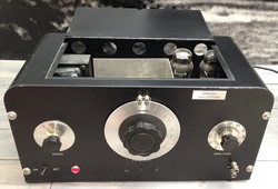
Figure 2 Fully functional HP200A audio oscillator, the first product offered by HP.
Building 1 on the sprawling campus includes an area commemorating the firm’s 75-year history, including a large wall listing each of the patents in their portfolio (see Figure 1) as well as displays of the test equipment that is their raison d’être. An HP200A audio oscillator – the product that launched HP – is fully functional, with glowing tubes and a red power light on the front panel (see Figure 2). It is joined by a progression of test systems produced over the years, with a large timeline that spans the hallway and commemorates the key events in the company’s history. Adjacent walls are decorated with stunning photos taken by employees, the winners of a monthly contest (see Figure 3).
STRATEGY
Keysight is focusing on three broad markets: 1) communications 2) aerospace and defense, and 3) industrial, computers and semiconductors. Each segment offers growth, from such drivers as mobile data, more connections, higher data rates and defense modernization. To broaden its product portfolio from the long-standing test and measurement “boxes,” Keysight is expanding its offerings in modular, software and complete system solutions.
One recent example of the latter is the collaboration between Keysight and Cascade Microtech to offer a wafer-level measurement system. This comprises all hardware and software as well as initial setup, calibration, training and service. Cascade provides a single point-of-contact for all technical support. This complete system solution was prompted when both companies noticed that many customers let these large capital items sit for months awaiting setup and qualification, simply because of a lack of manpower or missing accessories. So Keysight and Cascade Microtech teamed up to solve the problem and provide more value to their customers. They also developed a software platform, WaferPro Express, to automate on-wafer measurements and manage a device modeling database for data analysis, model extraction and verification.

Figure 3 Photos taken by employees hang on the walls at Keysight Technologies' headquarters in Santa Rosa.
To serve the rollout of 4G and adoption of heterogeneous networks, Keysight is developing products such as one-box testers like the UXM, for R&D, and EXM for manufacturing. With the Internet of Things (IoT) and 5G on the horizon, the company is engaged in industry research and standards development, which will define future test and measurement needs.
VERTICAL INTEGRATION
Keysight is known for high quality and high performance test equipment, which is a result of attention to detail at every step of design, manufacturing and test. Almost all of their microwave devices are produced in Santa Rosa, including GaAs and InP MMICs and YIG spheres. Their III-V wafer fab focuses on performance, reliability and long lifetimes, not volume. The fab runs about 2500 three-inch wafers per year across 13 processes that include MESFET, PHEMT and HBT devices. Keysight operates several MBE systems to tailor device epitaxy and optimize performance.
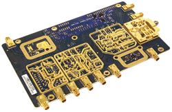
Figure 4 Integrated RF subassembly showing Keysight's chip-on-board technology. Connectorized thin-film modules, such as the one on the right side of the board, are used for circuits operating well into millimeter wave frequencies.
To support the unique needs of test and measurement equipment, they develop custom packaging solutions that include thin-film deposition, machining and sealing. Internal semi-automated and fully automated die-attach and wire bonding manufacturing lines serve both development and production.
A good example of Keysight’s RF expertise is the development of RF assemblies using a high performance, chip-on-board technology that can integrate an RF front end onto a single laminate board (see Figure 4). This packaging technology includes the capability to incorporate walls to shield sensitive RF circuits. A typical board is highly integrated, containing 35 to 40 RF devices and hundreds of other components. Compared with the traditional approach of thin-film circuit assemblies in machined and plated housings, the chip-on-board laminate reduces size, weight and cost while maintaining – even improving – performance.
The laminate board works to frequencies well beyond 26.5 GHz and traditional hybrid modules can be used in concert with the laminate to deliver performance far into the millimeter wave range. Modules can be mounted onto the laminate board, with the module RF signal connected to the laminate before or after frequency conversion. Figure 4 shows a high frequency module with a precision, ruggedized connector on the right side of the laminate board.
To automate the final testing of Keysight’s test and measurement equipment, five company engineers developed a robotic line that moves each instrument into and out of various test stations, tracking the test flow, measured data and pass/fail results. DC and RF connections to the unit under test are made automatically, and electrical tests can be performed at hot and cold temperatures. When a test is complete, the robotic cart returns to the station and moves the unit to the next test. Status and data are available online, allowing employees to monitor the results from anywhere. Two robotic lines run in Santa Rosa, and the company’s production facility in Malaysia has eight.
CULTURE AND STRATEGY
Management guru Peter Drucker is credited with coining the maxim “culture eats strategy for breakfast,” meaning a misaligned culture can undermine the best strategy. After a day walking the halls and speaking with numerous Keysight employees, we left Santa Rosa feeling that the people are proud, energetic and enthusiastic about the future – which makes the culture a strong and secure foundation for Keysight’s strategy. The energy and enthusiasm felt like a startup, yet one with a proud, 75-year history. A unique $3 billion startup has indeed been reborn.