

The ADF7242 is a low power, short-range transceiver designed for operation in the global 2.4 GHz ISM band. It complies with the IEEE 802.15.4-2006 2.4 GHz PHY requirements with a fixed net data rate of 250 kbps and DSSS-OQPSK modulation. Additionally with GFSK/FSK modulation, the ADF7242 supports a wide range of data rates, and is therefore equally suitable for proprietary applications. The agile frequency synthesizer of the ADF7242, together with short turnaround times, facilitates the implementation of FHSS transmission systems.
The ADF7242 has been designed with emphasis on flexibility, robustness, ease of use and low current consumption. The receive path is based on a zero-IF architecture enabling high blocking and selectivity performance. The transmit path is based on a versatile direct closed-loop VCO modulation scheme to allow the device to work with a variety of modulation schemes and data rates with a very low modulation error rate. The ADF7242 features an excellent performance versus power consumption metric, making it especially suitable for battery-powered systems.

The ADF7242 features a flexible dual-port RF interface with support for switched antenna diversity (see Figure 1). An integrated biasing circuit is also provided to significantly simplify the interface to external PAs. Its applications can include the areas of smart metering, industrial control, home and building automation, health care and consumer electronics.
Dual-mode functionality
The fact that the ADF7242 supports both IEEE 802.15.4 and GFSK/FSK modes allows a user to design a network that can incorporate both a standardized communications protocol and a proprietary link using one transceiver. For example, in a smart metering application the ADF7242 enables communications with standard ZigBee sensors in the home while meter information could be relayed in the neighborhood area network using a proprietary link.
RF performance
Receiver
The 2.4 GHz ISM band offers the advantage of being able to operate globally. However, this advantage means that it can be a busier/noisier environment. Thus, for robust and efficient operation, resilience to interferers is particularly important in this band. The value of good sensitivity and low current will be constrained if the reception is not successful, necessitating retransmissions in this real world environment. The zero IF architecture of the ADF7242 facilitates its robust performance in the presence of interferers. It does not suffer from the inherent finite image channel rejection of a low IF architecture. In IEEE 802.15.4 mode, for example, the ADF7242 can successfully receive in the presence of another IEEE 802.15.4 signal in either an adjacent channel, which is 48 dB higher or an IEEE 802.15.4 signal, which is two channels away and is 62 dB higher. With the signal level at -92 dBm reception is still successful when a CW interferer at 5 MHz offset from band edge is as high as -26 dBm.
Transmit
The transmitter has programmable output power from -20 to +4 dBm with good stability over supply and temperature. The transmitter incorporates a PA ramping controller, which minimizes spectral splatter generated by the transmitter. Upon entering the Tx state, the ramping controller automatically ramps the output power of the PA from the minimum output power to the specified nominal value. The ramp rate is user programmable. Particular emphasis has been placed on the versatility of the transmitter to support the IEEE802.15.4 standard as well as FSK or GFSK modulation schemes with data rates ranging from 2 Mbps down to 50 kbps. The transmitter typically achieves a 3 percent EVM in the IEEE802.15.4 mode and 8° RMS phase error in 2 Mbps GFSK mode at 3 dBm output power.
RF Port interface features
External PA Interface
For applications where higher output power is desirable, the ADF7242 offers an integrated biasing block for the external PA circuits. It is especially suitable for external PA circuits based on a single GaAs MESFET and a wide range of integrated PA modules. The key elements are a switch between pin VDD_BAT and pin PAVSUP_ATB3, a 5-bit DAC and a bias servo loop, all of which are controlled by control logic. This interface is enabled either under direct control of the MCU or automatically while the ADF7242 is in the Tx state.
Using this internal switch allows the supply to an external circuit to be switched on or off, which is useful for circuits that have no dedicated power down pin and/or have a high power-down current. In addition, the PABIOP_ATB4 pin can act as a programmable current source or sink.
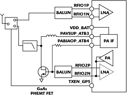
Figure 2 Typical external PA applications circuit.
When the PA circuit is based on a single external FET, the bias servo can be used to stabilize its output power by controlling the gate bias voltage of the external FET such that the current through the supply switch is equal to a reference current. The reference current for bias servo is generated by the current DAC (see Figure 2).
Dual RF Port: Configurations/Antenna Diversity
The ADF7242 is equipped with two fully differential RF ports. Port 1 is capable of receiving; Port 2 is capable of receiving or transmitting. Only one of the two RF ports will be active at any one time. The availability of two RF ports facilitates the use of switched antenna diversity. For receive antenna diversity, the link margin is maximized by selecting the optimum antenna based on the RSSI level of the desired signal received with each antenna. As an additional parameter, the measured link quality can be used. Suitable algorithms for the selection of the optimum antenna depend on the particulars of the underlying communication system. In a static communication system, it is often sufficient to select the optimum antenna once during setup.
The dual RF ports also simplify the application circuit if the ADF7242 is connected to an external LNA and/or PA. Connecting to an external PA and/or LNA is possible with a single external Rx/Tx switch, reducing the cost and loss associated with an additional switch. In addition to the external PA support described, the ADF7242 provides two signals to automatically enable an external LNA and/or a PA while in Rx or Tx state, respectively.

Figure 3 RF interface configuration options (A: Single antenna; B: Antenna diversity; C: External LNA/PA; D: Dipole antenna).
Figure 3 shows some of the different possible RF PORT configurations. In configuration A, a single antenna is connected to RF Port 2. In configuration B, a dual-antenna configuration is suitable for switched antenna diversity. In configuration C, the PA is configured to transmit on RF Port 2. RF Port 1 is configured as the receive input. Configuration D is similar to configuration A, except that a dipole antenna is used. In this case, a balun is not required.
Ease of use/Flexibility in data processing
In FSK/GFSK a sync word of up to 24 bits can be programmed and optionally be used to activate the SPORT interface on sync word detection in receive mode. In IEEE 802.15.4-2006 mode a total of 256bytes of TX_BUFFER and RX_BUFFER are provided to decouple the over-the-air data rate from the MCU processing speed. The integrated automatic packet handling includes the insertion of preamble, SFD and FCS in transmit and SFD detection and FCS checking in receive mode. Allowing additional flexibility, an alternative to the standard IEEE 802.15.4-2006 SFD byte can option≠ally be selected by the user and used by the ADF7242 packet handling processes. Additionally, a firmware download is available to control timing critical activities in IEEE 802.15.4-2006 mode. This includes address filtering, auto acknowledge and CSMA-CA.
In conclusion, the ADF7242 provides a flexible and robust solution for the 2.4 GHz ISM band market, incorporating dual-mode operation, excellent RF performance and a range of features to facilitate ease of use.
Analog Devices,
Norwood, MA
(800) 262-5645,
www.analog.com
RS No. 301