
Due to the fast development of wireless communications, a low cost, high performance, high integration technology is needed for system on a chip (SOC) implementation. The CMOS technology provides a good solution for SOC integration.1
Recent improvements of the standard CMOS process make it possible to implement RF blocks, such as low noise amplifiers (LNA), voltage-controlled oscillators (VCO) and mixers, for operating at frequencies up to 5 GHz.

However, the CMOS PA remains one of the most difficult blocks to implement due to the limited breakdown voltage, especially in advanced submicron CMOS processes.
It is a very challenging task to implement a high performance CMOS PA.
To improve the PA linearity, some linearization techniques, such as feedforward, feedback and predistortion have been developed, although they are not capable of being integrated in a single IC.
Due to its small size and lack of DC current consumption, the diode linearizer2,3 is a good choice to be integrated in the PA design.
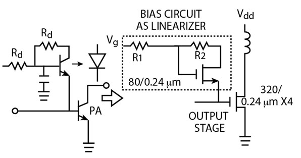
A similar technique using nonlinear capacitance cancellation in a CMOS PA design has been reported.4 The integrated diode linearizer, used in an HBT PA, can effectively improve gain compression and phase distortion performance by compensating the effects suffered from the gate DC bias level (Vgs), which decreases as the input power increases. A PA using an integrated diode connected NMOS transistor functioning as a diode linearizer is shown in Figure 1.
Figure 2 shows the time domain simulated results for a 320 µm wide, common source NMOS transistor without and with the linearizer, driven by input powers from -10 to 6 dBm (biased at Vgs = 0.8 V).

While the gate bias DC level of the transistor without the linearizer drops to 0.71 V (0.5 x (m1 + m2)) at an input power of 6 dBm, that of the transistor with the linearizer has almost no change and maintains a 0.8 V bias. This article presents the design of a 2.4 GHz CMOS PA using this technique, fabricated in a TSMC 0.25 μm 1P5M standard CMOS process.
PA Circuit Design
In the standard 0.25 μm 1P5M CMOS process, the NMOS transistor has a drain-source breakdown voltage of approximately 5.4 V and a knee voltage of approximately 0.5 V. With the limited 2.5 V drain DC supply voltage and a poor power handling capability, designers face a severe challenge when designing a CMOS power amplifier. To reach high output powers, above 20 dBm, designers must use large size NMOS transistors to implement a PA, although it will decrease the frequency response due to the increase in parasitics.
Figure 3 shows the schematic and layout of the two-stage PA with a chip area of 1100 x 700 μm2 including bonding pads. The output stage operates in class AB (near class B) to obtain high efficiency and the output transistor is 960 μm wide.

The input stage operates in class AB to offer enough power gain, and the size of the input transistor is chosen to be one third of the output transistor's size.
Because the metal-5 spiral inductors offered by the foundry are 10 μm wide and cannot carry a high current density, both of the RF chokes are placed off-chip. The diode linearizer is formed by a 80 μm wide diode-connected NMOS transistor and is placed in the output stage as the gate biasing circuit.
To avoid the loss of model accuracy, parts of the input and output matching networks are placed off-chip, but some matching information is kept in mind during simulation, including the effects of the FR-4 PCB test fixture and passive components. After the final tuning of the input and output matching networks using microstrip lines, the fabricated CMOS PA shows satisfactory performance in power gain and output power characteristics.

Due to the large size of the output stage transistor, it is split into two separate parts and placed on opposite sides. Figure 4 shows a photograph of the PA in an FR-4 PCB test fixture.
Measured Results
The measurements are performed on an FR-4 PCB test fixture. The PA chip is connected to the PCB test board with aluminum bond-wires. The equivalent model of the bond-wire is approximately 1nH/mm. The measured small-signal gain is 11.2 dB and the input return loss is 24 dB at 2.45 GHz, as shown in Figure 5.
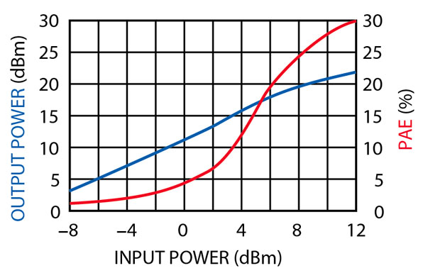
Figure 6 shows the measured output power and power-added efficiency (PAE) of the PA using the linearizer. It exhibits an output power of 20 dBm and a PAE as high as 28 percent.
To compare the biasing topologies in linearity characteristics fairly, the two biasing circuits are integrated in the same PA chip layout but work individually, such that two biasing circuits can share the same FR-4 PCB test fixture.
Figure 7 shows the measured gain compression. The gain compression of the PA using the diode linearizer is a little higher than that using the conventional biasing topology.

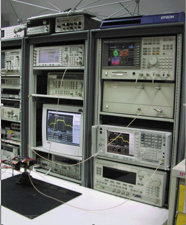
Figure 8 shows a photograph of the instrumentation set-up, including a vector signal generator, a vector signal analyzer and a spectrum analyzer, for error vector magnitude (EVM) and adjacent channel power ratio (ACPR) measurements in digital modulation tests.
Figure 9 shows the ACPR measurement of the PA with π/4 DQPSK modulation (data rate = 48.6 kbps channel spacing = 30 kHz channel BW = 24.5 kHz).
It shows a 2.2 dBc improvement in ACPR by using the diode linearizer. For ACPR measurements with different output powers, it can be seen that for most of the output power range, the ACPR with the diode linearizer is better than that with the conventional biasing topology (see Figure 10).
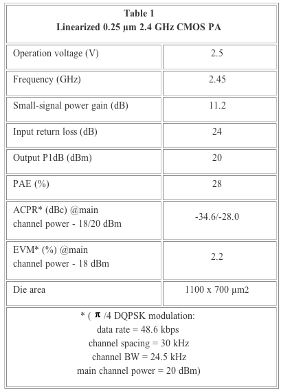
The EVM measurement of the PA, without and with the linearizer at a 18 dBm main channel power output, shows a slight improvement of 0.24 percent. The summary of the measured characteristics of a linearized 2.4 GHz CMOS PA are shown in the Table 1.
Conclusion
A 2.4 GHz CMOS PA integrated with a diode linearizer, fabricated in a TSMC 0.25 μm standard CMOS process, is presented. The integrated diode-connected NMOS transistor serves the function of a diode linearizer, which can effectively improve the linearity of the fabricated class AB output stage without increasing the chip size.
The designed PA reaches an output power of 20 dBm and a PAE of 28 percent. The ACPR and EVM measurement of the PA with π/4 DQPSK modulation (data rate = 48.6 kbps channel spacing = 30 kHz channel BW = 24.5 kHz, main channel power = 18 dBm) are -34.6 dBc and 2.2 percent, respectively.
It demonstrates the great potential of the standard CMOS process in designing and manufacturing a 2.4 GHz PA for Bluetooth and WLAN 802.11b applications.

Acknowledgment
The authors would like to thank the Chip Implementation Center (CIC) of the National Science Council, Taiwan, ROC, for supporting the TSMC CMOS process.
References
1. T.H. Lee, The Design of CMOS Radio-frequency Integrated Circuits, Cambridge University Press, New York, NY 1998.
2. T. Yoshimasu, M. Akagi, N. Tanba and S. Hara, "An HBT MMIC Power Amplifier with an Integrated Diode Linearizer for Low Voltage Portable Phone Applications," IEEE Journal of Solid-State Circuits, Vol. 33, No. 9, September 1998.
3. T. Yoshimasu, M. Akagi, N. Tanba and S. Hara, "A Low Distortion and High Efficiency HBT MMIC Power Amplifier with a Novel Linearization Technique for p/4 DQPSK Modulation," IEEE GaAs IC Symposium Technical Digest, 1997, pp. 45-48.
4. C. Wang, L.E. Larson and P.M. Asbeck, "A Nonlinear Capacitance Cancellation Technique and its Application to a CMOS Class AB Power Amplifier," IEEE RFIC Symposium Digest, 2001, pp. 39-42.

 Cheng-Chi Yen received his MSEE degree from National Cheng Kung University, Tainan, Taiwan, in 2002, where he worked on 2.4 GHz CMOS power amplifiers and RFICs for his master study. He currently works for the AIROHA Technology Corp. as an RFIC designer. His research interests include RFIC/MMIC design for wireless communication systems.
 Huey-Ru Chuang received his BSEE and MSEE degrees from National Taiwan University, Taipei, Taiwan, in 1977 and 1980, respectively, and his PhD degree in electrical engineering from Michigan State University, East Lansing, MI, in 1987.
From 1988 to 1990, he was with the Portable Communication Division of Motorola Inc., Ft. Lauderdale, FL. He joined the department of electrical engineering at National Cheng Kung University, Tainan, Taiwan, in 1991, where he is currently a professor.
His research interests include portable antenna design, RF/microwave circuits and RFIC/MMIC for wireless communications, electromagnetic computation of human interaction with mobile antennas, EMI/EMC, microwave communication and detection systems.