

A wideband unidirectional pattern antenna operating in the n258 band is realized on a low-cost, high dielectric constant substrate. The antenna is a multi-layer design, which achieves an impedance bandwidth of 13.6 percent centered at 26 GHz and has a peak gain of 6 dBi. To achieve hemispherical coverage, a multi-port electrically compact pattern diversity module is also investigated. The constituent antennas of the module maintain the impedance bandwidth. Isolation between ports is greater than 30 dB across the operational bandwidth.
The growth of smartphones in the recent decade demands that the hardware infrastructure facilitate these wireless nodes.1 These devices must be redesigned to accommodate future mmWave bands. The growth of carriers offering services in the sub-6 GHz bands indicates a trend toward migration to mmWave frequencies.2 Growth in the number of smartphone devices also means that the number of base stations catering to these smartphones must grow at a similar rate. Typically, the base station-to-smartphone ratio ranges from 1:300 to 1:500. Hence, optimization of base station antenna performance metrics is an important research objective.
With the introduction of new mmWave base stations, it is crucial to design systems that deliver optimal metrics in each geography. Migration to mmWave bands offers its own challenges and limitations. One of the major issues with mmWave carrier frequencies is inherent free space path loss (FSPL).2 For example, the free space path loss for a 100 m link designed on a 3.5 GHz ecosystem is 83 dB, while the FSPL at 26 GHz is close to 101 dB for the same distance.
To maintain the same link budget, the transmit power must be increased by 18 dB. This is challenging to achieve due to the limited power efficiencies of mmWave power amplifiers. The other alternative is to increase the gain of the antennas integrated with the transmitter terminals.
There are several approaches to enhancing mmWave antenna gain at the transmitter. A dielectric lens integrated with a unidirectional beam antenna would enhance the gain by 4 to 5 dB. The dielectric material used for this type of lensing action is expensive and challenging to assemble at mmWave frequencies. Parabolic reflectors or reflect arrays can deliver high gain with a pencil beam, but with a significant reduction in angular coverage. It must also be noted that these reflector-based radiating systems significantly increase the physical footprint of the radiating system, which may not be a suitable feature.
Many in the mmWave hardware industry believe that the most amicable approach to resolve the gain enhancement problem is to design phased arrays. Phased arrays can easily meet the desired specifications of the transmitter antennas, but with scanning loss in the range of 3 to 4 dB at ±45 degrees. This hampers its utility in the context of ceiling-mounted indoor base stations. The phased arrays must also be designed with the phase shifters and control circuitry.3,4
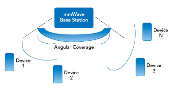
Figure 1 Typical 5G mmWave base station layout.
Another alternative is a pattern reconfigurable antenna with integrated pin diodes. This has severe power limitations along with the increased design complexity due to the biasing network near the radiating aperture.5
Hence, a beam switchable pattern diversity antenna module is proposed in this work (see Figure 1). Here, the high gain beam switching module is integrated within the base station, catering to numerous devices compliant with the 5G protocols. It is clear from the illustration that high gain and wide angular coverage are contradictory requirements. Hence, the proposed electrically compact antenna solution is a trade-off between high gain and wide angular coverage.
WIDEBAND ANTENNA ELEMENT
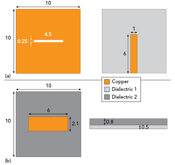
Figure 2 Antenna schematic: feed (a) and radiating patch (b). Dimensions are in mm.
To realize a multi-port antenna system, the unit element must be designed such that it operates within the intended n258 band with a high front-to-back ratio and high gain for the available radiating aperture. The antenna is an aperture-coupled element with two different dielectric substrates (see Figure 2).6
The feed substrate is shown in Figure 2a. The feedline is matched to the impedance of the radiating patch through a non-radiating slot in its ground plane. The lower substrate is industrially viable, low-cost FR4, which has a thickness of 0.5 mm, a dielectric constant of 4.4 and a loss tangent in the range of 0.03 to 0.04. The substrate is electrically thin at the desired operating frequencies. It is 10 × 10 mm to accommodate the connector for measurement purposes, but it could be marginally larger than the radiating patch.
The patch (see Figure 2b) is optimized to radiate in the 26 GHz band. It is designed on a thicker substrate than the feed to enhance its impedance bandwidth. Bandwidth could be further increased by choosing a 1.6 or 3.2 mm substrate. However, the dielectric losses would hamper the antenna’s broadside gain.
The prototype antenna is shown in Figure 3. Standard commercially available photolithography techniques were used to individually fabricate both layers. CNC machining was used to profile the substrates. The feed line is extended 5 mm to accommodate the solderless end-launch connector. The radiator is spaced greater than 10 mm from the electrically large connector to avoid any effects of the connector on the measurements. The substrates are bonded with an electrically thin adhesive.
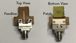
Figure 3 Photograph of the fabricated prototype antenna element.
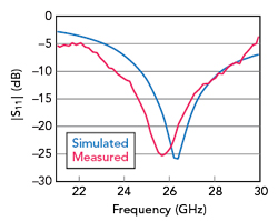
Figure 4 Antenna element input reflection coefficient.
Simulated and measured |S11| are shown in Figure 4. The -10 dB operational bandwidth is 3.6 GHz from 24.7 to 28.3 GHz, or 13.6 percent for operation in the n258 5G band. The broad impedance bandwidth could be attributed to the use of multiple dielectric layers. Bandwidth could be further increased by redesigning the patch with an electrically thicker substrate, but this approach would reduce the gain.
Simulated and measured principal cut antenna patterns at 26 GHz are shown in Figure 5. Beamwidth is 135 degrees in the E-plane and 71 degrees in the H-plane. The front-to-back ratio is greater than 15 dB across the operating band; this could be attributed to the non-radiating ground plane beneath the radiating patch. Asymmetry of the beamwidth in the principal planes could be attributed to the optimized geometry of the overall dielectric. Because the antenna element provides a unidirectional beam with a high front-to-back ratio, it could be used to construct a diversity module with a wide angular coverage pattern.
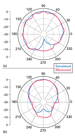
Figure 5 Antenna element principal plane patterns: elevation (a) and azimuth (b).
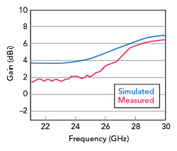
Figure 6 Antenna element gain.
The broadside gain of the antenna is shown in Figure 6. It achieves a peak gain of 6 dBi in the n258 band. The antenna’s high gain is due to the non-radiating ground plane in the feed design and is sufficient to construct a three-port antenna module with a physically small footprint.