


The complexity of RF circuits and systems, coupled with stringent performance targets, has made simulation essential. Historically, simulations were configured and run manually, with engineers reviewing results and deciding next steps. More recently, Python-based automation has emerged as a compelling alternative, improving efficiency, scalability and repeatability. However, many RF engineers do not consider themselves programmers, making it difficult to translate their deep design expertise into workflows built entirely in code.
A new paradigm is emerging for orchestrating RF simulations. This methodology trades pure code-based automation for an executable visual flowchart. Yet it doesn’t eliminate Python from the picture. Instead, the approach spans no-code, low-code and fully coded orchestration, adapting to both requirements and individual preferences. Combining Python with a visual flowchart offers the best of both worlds: humans can quickly understand the logic, while decision-making can be handed off to agentic AI.
We will demonstrate the benefits of a flowchart-based approach using an RF power amplifier (PA) design example and the technique of intrinsic node waveform engineering. This approach integrates common simulation tasks, including DCIV, S-parameter extraction, load- and source-pull analysis, harmonic balance (HB), parameter sweeping and optimization, into a single executable flow. Finally, we will discuss how AI can fit into this workflow through surrogate modeling, natural language prompting and agentic decision-making.
RF WORKFLOW ORCHESTRATION – A NEW FLOWCHART PARADIGM
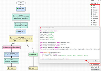
Fig. 1 A Nexus Connect flowchart and its associated Python code.
Like many software applications, RF simulators began with command-line interfaces and later evolved into graphical user interfaces (GUIs). Dialog boxes are typically intuitive, with features such as buttons, checkboxes, drop-down menus and short text fields. The learning curve is short, but GUIs have downsides. For example, achieving consistent results across ad hoc simulation runs requires that all fields be entered in exactly the same way every time. Reusable simulation templates can help, but since they are usually editable, traceability remains elusive. Another major limitation of GUIs is scalability: as circuit complexity and the number of design variables increase, manual editing becomes impractical.
Scripting improves the situation by fostering repeatability and enabling scalability. Many RF software tools began adding programmability through various (sometimes proprietary) scripting languages. Then Python burst onto the scene, growing into the world’s most popular programming language. Some EDA vendors began efforts to retool around Python, benefiting from its vast ecosystem of open-source libraries and improved code portability and reuse.
Keysight leaned into the trend by adding Python support to its existing software platforms, including Advanced Design System (ADS). Simultaneously, research and development was underway on a next-generation, Python-native platform called RF Circuit Simulation Professional (Nexus), which has now been released and is available to customers. Nexus is designed with automation and AI-readiness in mind.1
Building on Nexus, Keysight is taking a new step in reimagining RF design workflows. Nexus Connect represents a new paradigm, enabling individuals and organizations to capture their design engineering processes as flowcharts, similar to how measurement processes are captured with visual tools. As shown in Figure 1, the flowcharts comprise various action blocks, or “steps,” underpinned by modifiable Python code. The flowchart manages tasks and decisions, allowing pre-planned, orchestrated workflows to run automatically and be reproduced precisely.
Visual flowchart diagrams help engineering teams capture and share information. From the moment a design project begins, engineering thinking becomes transparent and is saved electronically rather than lost when a physical whiteboard is erased. Instead of leafing through tedious documentation or tracking down colleagues, team members at any skill level can immediately see the types of simulations and parameters chosen, the goals used for optimization and the criteria for deciding how to proceed based on the results. Diagrams can also serve as the focal point for design reviews. New designs can start with reusable diagrams. The time savings from improved orchestration and reduced workflow friction add up quickly.
PA DESIGN WITH AN INTRINSIC NODE MODEL AND WAVEFORM ENGINEERING
The best way to illustrate this is with a real‑world example. Here, we focus on RF PA design, specifically a Class J amplifier, which is similar to Class B operation but uses harmonic tuning to improve efficiency. The complexity of PA design makes it an ideal vehicle for discussing workflow orchestration. This discussion is kept at a high level so that all RF designers can follow along, not just those specializing in PAs. In this example, ADS is used for schematic capture and data display, and Nexus to run simulations.
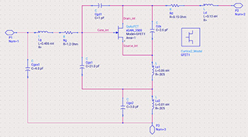
Fig. 2 An intrinsic-node GaN transistor model with a current generator and parasitics, represented in ADS.
Much has been written about extrinsic design methodologies for PAs, in part because they align with how designers measure and characterize circuits. This approach places the reference plane for simulations or measurements at a physically accessible boundary — typically the transistor terminals, either at the package leads or at the die edge. As a result, an extrinsic model or measured dataset inherently includes the parasitic resistance, capacitance and inductance present within the device.
In contrast, intrinsic design methodologies analyze voltages and currents at internal device nodes rather than at terminals. By working closer to the intrinsic current generator, designers can directly observe waveforms that are typically masked by device parasitics. This perspective provides deeper insight into transistor operation and enables the evaluation of key PA performance metrics. Figure 2 shows a schematic of a conceptual, non-process-specific GaN transistor with its intrinsic device nodes explicitly exposed.
Access to intrinsic nodes allows PA designers to build circuits around first principles. The challenge with implementing an intrinsic-node method is that many manual steps are required to iteratively optimize a design.2
- Ideal nonlinear voltage and current waveforms are superimposed on a device’s DCIV curves to determine the power and efficiency a device could achieve in that operating state.
- Strategically engineered waveforms reduce overlap between the time-domain voltage and current waveforms, minimizing resistive power dissipation.
- The Class J mode tunes the second-harmonic load impedance to boost the voltage waveform, while higher harmonics shape the current waveform, theoretically allowing an efficiency of 78.5 percent with a more flexible set of harmonic impedances than in Class B.
- The time-domain waveforms are then transformed into the frequency domain using an FFT, yielding computed impedances at the fundamental and harmonic frequencies.
- The time-domain waveforms are then transformed into the frequency domain using an FFT, yielding computed impedances at the fundamental and harmonic frequencies.
- By applying those impedances back to the idealized current generator in the intrinsic-node transistor model, energy organizes into the efficient waveforms we started with, maximizing achievable device power efficiency.