


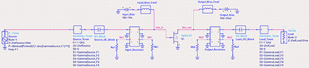
Fig. 3 PA design bench schematic in ADS using the GaN FET model.
The PA design bench schematic in ADS, as seen in Figure 3, mimics a load-pull measurement system.3 It includes harmonic tuners, bias networks and receivers for the A (incident) and B (reflected) waves, enabling a complete analysis of PA metrics. The device under test (DUT) is the GaN FET model shown in Figure 2.
A single Nexus Connect task captures the sequence of analyses and tasks required to complete a significant portion of a Class J amplifier design. Figure 4 shows the first few steps of the Nexus Connect executable flowchart.
- First, the task performs a DCIV sweep, followed by load-line calculations for bias and target intrinsic impedances (Zs) at each harmonic.
- Then, it sequentially optimizes extrinsic loads for each harmonic to achieve the target intrinsic Zs.
- Next, it performs a source-pull analysis and an input power adjustment to match power and efficiency.
- Then, an S-parameter analysis is performed, including stability calculations with Winslow virtual probes.
- Finally, a power-swept HB analysis confirms the overall PA performance.
As the flowchart execution graph progresses, run blocks can change color (a programmable setting) and double-clicking a block can reveal simulation or optimization results. Figure 4 also shows a portion of the optimization results from the first load-pull analysis when the graph is clicked.
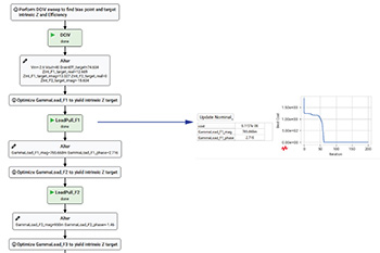
Fig. 4 A Nexus Connect task execution flowchart with results of a load-pull optimization displayed.
Designers can set top-level parameters such as the target output power, alpha (which reshapes the voltage waveform and changes the target impedances without affecting power or efficiency) and the percentage of the device’s maximum output current for the quiescent (q) point. Re-running the flowchart with new top-level parameters produces updated results quickly (in less than a minute on a laptop).
Deriving target intrinsic gammas involves constructing a load line from the DCIV sweep data by connecting the q point to one of the knee points. First, simple Python algorithms and heuristics determine the q point from the device’s breakdown voltage and the desired output current at cutoff (a small percentage of the maximum output current). Then, knee points are calculated for all simulated Vin curves, as shown in Figure 5.
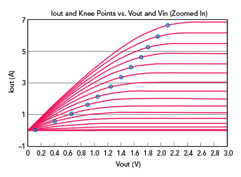
Fig. 5 DCIV sweep data plotted with all the calculated knee points.
Next, load-line metrics are evaluated for all knee/quiescent point pairs, and additional Python algorithms are used to select a load line from the candidates. The algorithms balance output power and efficiency while walking down the knees. (The actual details of our algorithms are not the focus here — the key point is that all decisions and rules are formally captured in the execution flowchart.) The blue line in Figure 6 is the rectified load line (or IV swing at alpha equals 0.0). With the FET biased for Class J operation at the q point, the instantaneous current and voltage swing along the line when an RF signal is applied. The FET conducts zero current for half of the RF cycle, yielding a 50 percent duty cycle. With an alpha of 0.0, the voltage waveform is a pure sinusoid. Using alpha values of 1.0 or -1.0 gives a “harmonic boost” to the voltage waveform, moves the target intrinsic gammas off the real axis of the Smith chart and widens the IV swing trajectory away from the rectified load line shown in teal.
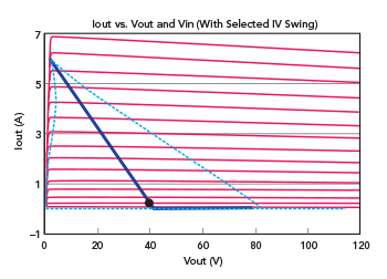
Fig. 6 IV swing trajectories for alphas 0.0 (blue) and 1.0 (teal) and q point (black), calculated from DCIV sweep data.
Once the Nexus Connect task is complete, we achieve a good match between the simulated and predicted intrinsic voltage and current waveforms, as well as the power and efficiency, as shown in Figure 7.
Extrinsic gammas, which are ultimately needed for matching network design, differ from intrinsic gammas because of the parasitics in the device model. The Nexus Connect task sequentially optimizes the extrinsic gammas up to the fifth harmonic, see Figure 8, to minimize errors in achieving the target intrinsic gammas.
The entire sequence shown, comprising simulations, algorithms and decisions, is captured and executed in a single Nexus Connect flowchart. While an engineer could have initiated the same steps manually via the Nexus graphical user interface, it would be hard to reproduce the exact repeatable steps from separate, disconnected analyses and tasks.
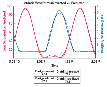
Fig. 7 Simulated (solid) versus predicted (dashed) intrinsic waveforms, output power and efficiency.
APPLYING AI FOR ADVANCED MODELING, ANALYSIS AND OPTIMIZATION
By capturing engineering processes, designers create well-defined interfaces that future AI tools can directly leverage. In AI-enabled workflows, agents are software programs that can operate autonomously, while skills are well-defined sets of instructions that agents or large language models (LLMs) can invoke to perform specific tasks. Diagramming the engineering workflow step by step gives engineers straightforward ways to use agents and skills productively. For example, an AI agent might extend the prior workflow to characterize all available transistors in a given technology and identify which devices perform best for a set of requirements. The agent or LLM might use a skill that describes how to set up and run a DCIV sweep and calculate the Class J load line. As AI tools evolve, these parts of the engineering process will converge, giving designers greater capabilities.
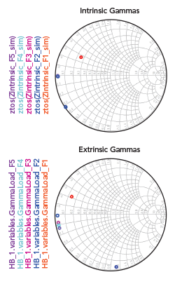
Fig. 8 Intrinsic and extrinsic gammas at each harmonic.
The waveform engineering orchestration in this example is only a small part of the larger PA design process. The prior workflow characterized the external impedances required at the device’s output node to achieve textbook Class J waveforms. Its output might be a table of impedances at the fundamental and harmonic frequencies, which, when presented to the transistor, yield efficient device operation. The next step is to design a matching network that presents these impedances to the device. Rapidly evolving AI capabilities will likely streamline this process. For example, surrogate models backed by artificial neural networks (ANNs) could reduce or eliminate computationally intensive electromagnetic (EM) simulations and even enable on-the-fly synthesis of physical structures.
Surrogate modeling involves an upfront, sometimes resource-intensive training process that requires extensive characterization (for example, EM simulations). Once training is complete and validated, simulations and optimization using physical structures become ultra-fast, making surrogate models strong candidates for AI-enabled or fully autonomous design. Surrogate approaches have received considerable attention in recent years because they can synthesize non-traditional, QR-code-like physical structures with well-behaved frequency responses.4 Recent research has even demonstrated the potential of such structures for harmonically matching a PA, as this example requires.5 Note that surrogate modeling is not limited to pixelated structures; it can work for any parameterizable physical structure, even an inductor.