

The increasing complexity of wireless communication systems necessitates careful optimization of noise performance, linearity and power efficiency in RF front-end designs. Among various silicon technologies, SiGe heterojunction bipolar transistors (HBTs) have emerged as the most compelling choice due to their superior high speed characteristics and well-controlled base parasitics. Their high transition frequency fT and inherently low base resistance enable excellent noise behavior, making them particularly suitable for low noise, high-linearity applications. Owing to these advantages and their scalability, bipolar devices continue to serve as key building blocks in silicon-based RF front ends.
The proposed high performance SiGe HBT double-balanced down-conversion mixer integrates several advanced design techniques to enhance overall performance. A transformer-free single-ended-to-differential conversion network is employed to improve efficiency and eliminate bulky passive components at the RF input. To further enhance linearity, a dual-feedback linearization strategy is implemented, simultaneously optimizing impedance matching and minimizing harmonic distortion. In addition, a symmetric device layout combined with multilayer PCB technology effectively suppresses LO-to-RF feedthrough, reducing crosstalk and improving port isolation. Collectively, these design strategies yield a highly linear, low noise and power-efficient mixer architecture, establishing a new performance benchmark for SiGe HBT-based mixer implementations and offering a robust alternative to conventional CMOS-based solutions.
INTRODUCTION AND CIRCUIT ANALYSIS
The active mixer uses a differential transistor as a current switch. The base voltage controls DC current flow from the collector to the emitter. By switching the base voltage at the LO frequency, while the small-signal RF is present in the inverted DC signal, the two signals will multiply. Gain is achieved by amplifying the RF signal (voltage-to-current conversion) before switching. The pre-amplification of the RF signal improves the signal-to-noise ratio (SNR), reduces the impact of noise and distortions introduced by switch losses and simplifies the input voltage-to-current conversion.
The proposed circuit is shown in Figure 1. The double-balanced mixer combines RF and LO signals while minimizing LO leakage at the IF output. This is achieved using two cross-coupled single-balanced networks that cancel in-phase and out-of-phase LO components before the current-to-voltage conversion stage. For analysis purposes, we can divide the circuit into two halves, each representing an identical single-balanced mixer network. The first left-half circuit consists of Q1 at the RF stage, with Q2 and Q3 serving as the switching cores. In the second half circuit, Q4 is at the RF stage and Q5 and Q6 are LO switching cores.
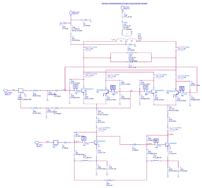
Figure 1 The architecture of a wideband double-balanced down-conversion mixer.
The single-balanced bipolar transistor (BJT) mixer utilizes transistor nonlinearities to perform frequency conversion by mixing an RF signal (vRF) with a local oscillator (vLO). In this circuit (Figure 1), transistor Q1 modulates its collector current based on the RF input. The LO signal drives the differential pair (Q2 and Q3) in a push-pull configuration, alternately steering the modulated collector current of Q1 between the two branches. This produces a differential output current (i2-i3) that comprises the sum and difference frequency components (fLO±fRF). The differential output current iout is expressed in Equation 1.
Here, the tanh term captures the saturating behavior of the LO differential pair. The large signal component, iRF, does not affect the output current. The double-balanced mixer effectively rejects the DC bias current component at the IF port, depending on current matching in the branches, load matching and the common-mode rejection of subsequent stages.
A down-conversion double-balanced Gilbert Cell Mixer with single-ended RF input and a fixed IF-tuned circuit with differential output at 145 MHz is presented in this work. The LO frequency sweep is from 355 to 1855 MHz and is fed differentially to the four LO transistors. The mixer is designed for a frequency range of 500 to 2000 MHz, and the RF signal is fed differentially (single-ended-to-differential conversion) to the RF transistor, as shown in Figure 1. This circuit consumes roughly 80 mW of power (supply voltage 4 V and total current 20 mA). The LO mixing core and RF stages are designed using Infineon high-linearity NPN SiGe BFP640 transistors and low noise NPN SiGe BFP840 transistors, respectively.
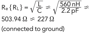
At the output, a fixed IF frequency of 145 MHz, a parallel-tuned circuit is used as a load between the differential outputs. Due to the high impedance, the mixer’s gain is maximum at its resonant frequency. The load impedance RL of the tuned circuit is computed by determining the real part of RL at resonance. Therefore, Equation 2 is true.
So, the total real part of the load can be expressed as Equation 3.
A step-down transformer is used to combine the differential output at the IF port and match it to the 50 Ω output.
Each RF stage comprises multiple feedback loops to adjust for transistor nonlinearity. In addition, series feedback from the second stage to the first stage corrects the phase shift between the two RF currents, thereby improving the mixer’s dynamic range. Each RF stage uses “dual-feedback linearization” to stabilize the current, with series inductive feedback at the input port and shunt resistive feedback at the output port controlling the output voltage, improving the transistor’s nonlinear transfer characteristics and reducing voltage distortion.1,2
Because of series feedback, the mixing circuit is less affected by source impedance. It enhances input impedance matching, reducing RF stage noise and increasing the input SNR. The shunt feedback minimizes noise at the output and lowers the output impedance, making it easier for the circuit to match the load. Enhanced linearity, a higher distortion-free dynamic range and a low noise figure were the outcomes of the combination effect of series and shunt feedback. The design optimizes conversion gain, noise figure, linearity and dynamic range at 1000 MHz RF frequency and 145 MHz fixed IF frequency.
RF port differential driver optimization is the most important trade-off. Here, a complex workaround is utilized in place of costly, potentially asymmetrical transformers like those found in diode mixers. The proposed approach involves a pre-driver stage that converts a single-ended line to a balanced line. As shown in Figure 1, the circuit employs a 180-degree phase shift in the first RF stage transistor to drive the second transistor. In ideal theory, the first RF common-emitter stage introduces a 180-degree phase shift between the base and collector. At the second step, the base-collector phase shift will be reset to zero degrees. However, the phase shift between two transistors is never completely optimal.
The gain of the second RF stage is gm times higher than that of the first RF stage. Balanced differential signal pairs convey signals with the same amplitude but a 180-degree phase change. If differential signaling is not properly balanced, it can cause interference or crosstalk,3 resulting in common-mode noise or voltage at the IF port. As a result, the gain at the second RF stage must be reduced to match the first stage’s performance. This can be accomplished by emitter degeneration in the second RF stage. With the specified impedance, both RF stages are emitter-degenerated, enhancing input stage linearity while also providing noise and power matching.
A: CONVERSION GAIN
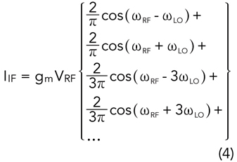
Figure 1 shows that the double-balanced mixer uses two voltage-dependent current sources. Moreover, both current sources have equal bias currents; the IF port current switches between gmVRF and -gmVRF. The DC biasing current Ibias is balanced because it always flows through both loads. As a result, the differential output voltage VIF is unaffected by the biasing current. The IF port current can be described in Equation 4.
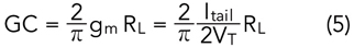
The voltage conversion gain of a double-balanced down-conversion mixer is the ratio of the output amplitude to the input amplitude and can be written as Equation 5:
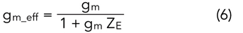
For the emitter degeneration case, the effective transconductance gm can be written as shown in Equation 6.
while emitter degenerating impedance ZE can be found using Equation 7.
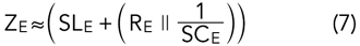
with the calculated value of ZE ≈ 21.983+j19.577 and |ZE | ≈ 29.436 Ω.
From Equations 2 and 3 the total real part of
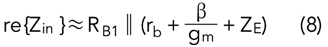
The input impedance Zin of the double balance mixer at RF frequency, looking into the base of the RF transistor Q1, is determined by the feedback element RB1 and the degenerative impedance ZE. Therefore, Equation 8 is true,
and the effective transconductance g m_eff at the mixing frequency of 145 MHz is 0.182 S and is shown in Figure 2.
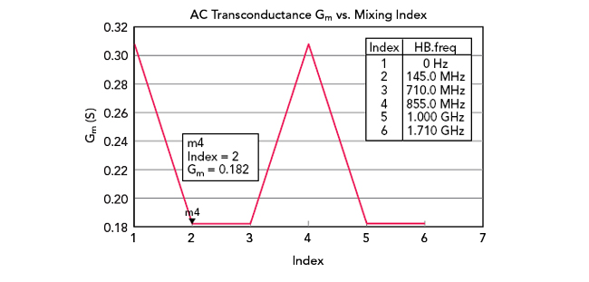
Figure 2 AC transconductance of the BJT Mixer.
So, the voltage conversion gain can be expressed by Equation 9.
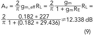
The measured value was about 12.64 dB.
B: TOTAL MIXER NOISE DOWN-CONVERTED TO THE IF PORT
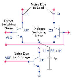
Figure 3 The primary noise sources in the single-balanced mixer.
The presence of noise in nonlinear circuits presents a complex challenge that requires careful analysis. Noise sources are typically considered to be stationary in linear circuits.4,5 The noise produced by a mixer exhibits periodic variation. The resulting noise processes are classified as cyclo-stationary,6,7 in which the dominant noise sources are switched on and off by the local oscillator. Figure 3 depicts the key mechanisms that contribute to noise, emphasizing the principal sources and outlining a basic approach for calculating noise spectral densities in a single-balanced mixer. The overall noise figure is determined by aggregating both linear noise sources and those influenced by the circuit’s periodic and time-varying characteristics.8,9