


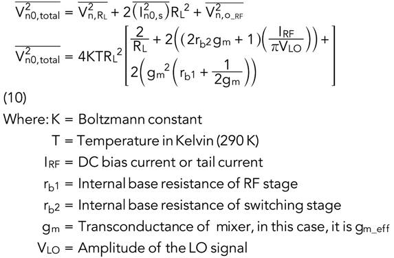
In a double-double-balanced mixer, the noise contribution at the intermediate frequency (IF) port is doubled as a result of the presence of two transconductance stages and switches. An in-depth examination of the mixer noise sources and their contributions to the IF port is presented by T. Kared.1 The total noise at the mixer output can be expressed as Equation 10.
Therefore, the input referred noise of the given mixer is shown in Equation 11.

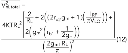
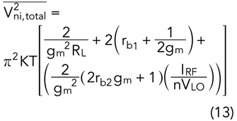
Substituting Equation 10 into 11, we get Equations 12 and 13.
So, the single-sideband noise figure SSB10 can be given as Equation 14.

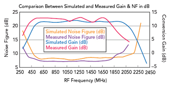
Figure 4 Comparison between simulated and measured data as a function of the RF frequency.
The IF spectrum will not contain any image frequencies due to the selectivity of the 145 MHz IF filter at the IF port. The resulting noise figure is single-sideband (SSB), not double-sideband (DSB). Figure 4 shows the simulated and measured conversion gain and noise figure as functions of RF frequency. The measured results exhibit a conversion gain of 12 dB ± 1 dB and a noise figure of 7 dB ± 0.4 dB over the frequency range of 600 MHz to 1.8 GHz, while the simulated results show a conversion gain of 11.4 dB ± 0.5 dB and a noise figure of 8 dB ± 0.2 dB across 500 MHz to 2 GHz. The IF frequency is down-converted to 145 MHz. Thus, the LO frequency is 145 MHz below the RF frequency. The LO balun frequency response determines the LO bandwidth. The LO and RF signals are AC-coupled via a coupling capacitor, which determines the lower frequency limit. At higher frequencies, parasitics (primarily substrate capacitance) from the board layout are prevalent and cannot be accurately modeled. This is the main reason the measured gain and noise figure bandwidth are lower than the simulated values.
From Figure 4, the measured noise figure of the mixer is lower than the simulated value. According to Friis’ formula, the input stage dominates the overall noise figure, with later stages contributing less. The mixer’s total noise mainly depends on each transistor’s internal base resistance and transconductance of each device; higher base resistance increases thermal noise and degrades SNR. Lower base resistance thus improves noise performance. The discrepancy between measured and simulated results likely arises from modeling inaccuracies and conservative SPICE parameter data in the ADS simulator, which limit simulation accuracy.
C: LINEARITY
The dynamic range of the mixer limits most communication systems. The linearity of the mixer relies on the RF transconductance stages, the LO switches and the tail current source. If the LO switches are ideal, the impedance observed at the emitters of Q2 and Q3 corresponds to that of the common-base stage, i.e., 1/gm2,3.11 The voltage gain at the collector terminal of Q1 is minimal, i.e, gm1/(gm2,3); therefore, the input third-order intercept point (IIP3) of the mixer is governed by the RF transconductance stage Q1, rather than the LO switching core.11 Since only the RF signal should be fed back to linearize the RF stage, the LO and IF signals should be minimized at the RF port to maintain port-to-port isolation. The collector currents of Q2, Q3, Q5 and Q6 are combined such that the RF and LO signals cancel at the IF ports. Applied feedback exclusively linearizes the RF stages; however, it does not affect the mixing stages. Concurrently, shunt-voltage feedback (Figure 1) is established between the collector of Q1 and the RF signal port node via resistor RB1.The analysis uses a large signal and the Ebers-Moll equation.
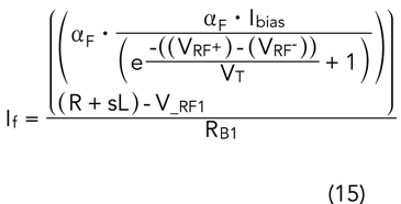
Equation 15 indicates that there are no terms involving the LO and IF signals. As a result, this current can be fed back to the input RF to help linearize the RF stage. The subsequent derivation shows that undesired signals are canceled at the IF port, as expected from the series feedback equation. Therefore, dual-feedback can be employed to improve circuit linearization. The detailed derivation of Equation 15 is provided by T. Kared.1
Figure 5 shows the measured compression characteristic of the down-conversion double-balanced mixer as a function of RF input power. Here, fLO=855 MHz and fRF=1000 MHz, and the RF power increases in each measurement. The mixer exhibits an uncompressed gain of about 10.79 dB, which drops by 1 dB at an input power of -8 dBm.
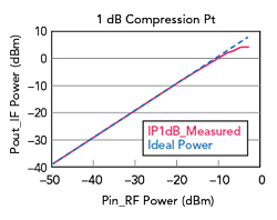
Figure 5 Measured compression characteristic of the down-conversion double-balanced mixer prototype.
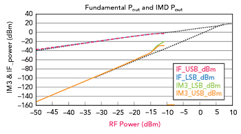
Figure 6 Extrapolation of the IP3 point at an RF frequency of 1 GHz.
Figure 6 illustrates the two-tone intermodulation test results used to determine the IIP3 and output third-order intercept point (OIP3) of the down-conversion double-balanced mixer prototype. The x-axis represents the applied RF input power (dBm), while the y-axis shows the corresponding IF output power (dBm). The red curve denotes the fundamental IF output power, which increases linearly with the RF input up to the compression region. The orange curve represents the third-order intermodulation (IM3) products, which rise at approximately 3x the rate of the fundamental tone. The linear extrapolations of both lines intersect at the IIP3 point, marked on the plot.
To determine the mixer’s IIP3, two input tones at 999.95 and 1000.05 MHz, each with a power level of -30 dBm, were applied. A 3 dB power divider separated two RF tones, producing IF outputs at 144.95 and 145.05 MHz, with third-order intermodulation products at 144.85 and 145.15 MHz. The third-order intercept point can be calculated using Equation 16.

Where Pin=-30 dBm and ΔP=Pout-P IM3
Now, for a lower sideband tone, ΔP=Pout-PIM3=-21.93-(-90.11)=68.18, therefore IIP3_LSB=4.09 dBm. For the upper sideband tone, ΔP=Pout-PIM3=-21.73-(-91.13)=69.40, so IIP3_USB=4.7 dBm. The OIP3 point is simply IIP3+Gain, which results in an approximate calculated OIP3 point of about 15 dBm.
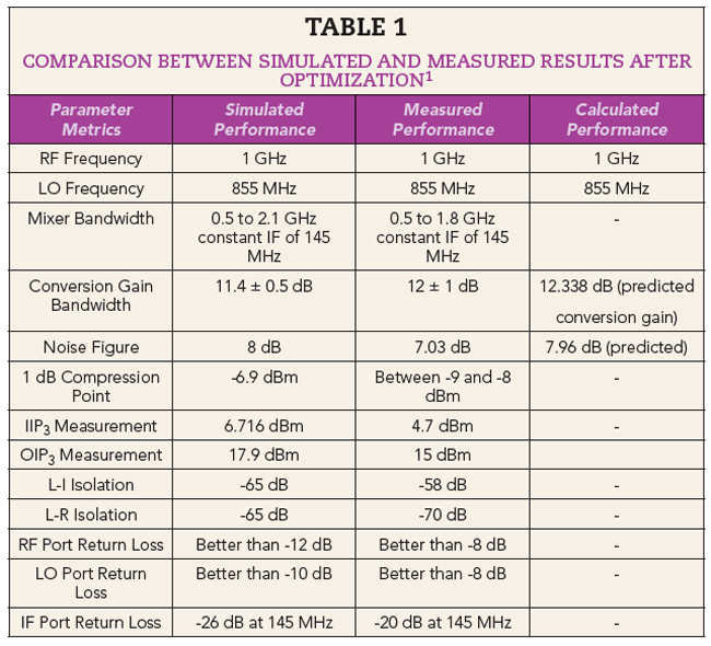
The noise floor of the circuit is about -166 dBm. The IP3 and 1 dB compression points are roughly 5 dBm and -8 dBm, respectively, so the available dynamic range can be calculated as (-174 dBm - 1 dB compression point + NF). This yields approximately 159 dBm/Hz for the available dynamic range. Table 1 compares the simulated and measured parametric performance of the down-conversion double-balanced mixer.
CONCLUSION
A new approach to designing a double-balanced mixer without the need for a bulky transformer at the RF stage is presented in this work. By implementing the dual-feedback linearization technique here, the voltage and current at the RF stages can be linearized, improving the nonlinear transfer characteristics and increasing IIP3 and the 1 dB compression point while maintaining a noise of about 7 dB and a gain of about 12 dB.
ACKNOWLEDGMENTS
This research, conducted as part of Trusha Kared’s Ph.D. dissertation, was carried out under the distinguished supervision of Prof. Dr.-Ing. habil., Ulrich L. Rohde, Prof. Dr.-Ing. Matthias Rudolph and Prof. Dr.-Ing. Ignaz Eisele (EMFT-Fraunhofer München, UniBW), in collaboration with Synergy Microwave Corporation and the Brandenburg University of Technology. The dissertation embodies a rigorous integration of theoretical development and experimental innovation in high frequency circuit design. Its significance was further recognized through a presentation at the Massachusetts Institute of Technology (MIT) Microsystems Technology Laboratories (MTL), highlighting its contribution to advancing state-of-the-art RF and microwave engineering research.
References
- T. Kared, “Mathematical Analysis, Design, and Validation of a High Dynamic Range, Low Noise Differential Mixer using SiGe Microwave Transistors,” 2025, Web: https://doi.org/10.26127/BTUOpen-712.
- T. Kared, H. Silaghi, M. Rudolph, A. Silaghi and U. L. Rohde, “Design of a Fixed IF Down-Conversion Double-Balanced Mixer for UHF Band Applications,” Sensors 2025, 25, 608, Web: https://doi.org/10.3390/s25030608.
- “The Advantages of Differential Signaling,” Cadence, Web: https://resources.system-analysis.cadence.com/blog/msa2021-the-advantages-of-differential-signaling.
- U. L. Rohde and M. Rudolph, “RF/Microwave Circuit Design for Wireless Applications,” John Wiley & Sons, Hoboken, N.J., Second Edition, 2012.
- G. D. Vendelin, A. M. Pavio and U. L. Rohde, “Microwave Circuit Design Using Linear and Non-Linear Techniques,” John Wiley & Sons Inc., Second Edition.
- J. Roychowdhury, D. Long and P. Feldmann, “Cyclostationary Noise Analysis of Large RF Circuits with Multitone Excitations,” IEEE Journal of Solid-State Circuits, 33(3):324-336, March 1998.
- W. A. Gardner, “Cyclostationary in Communication and Signal Processing,” IEEE, Piscataway, N.J., 1993.
- C. D. Hull and R. G. Meyer, “ A systematic Approach to the analysis of Noise in Mixers,” IEEE Transactions on Circuits and Systems, 40(12), December 1993.
- H. Darabi and A. A. Abidi, “Noise in RF-CMOS Miners: A Simple Physical Model,” IEEE Transactions on Solid-State Circuits, Vol. 35, No. 1. January 2000, pp. 15-25.
- B. Razavi, “RF Microelectronics,” Prentice Hall Inc., New Jersey, 1998.
- R. G. Meyer, “Intermodulation in High-Frequency Bipolar Transistor Integrated-Circuits Mixers,” IEEE Journal of Solid-State Circuits, SC-21(4):534-537, August 1986.