
An oscilloscope is used to capture the time-domain incident and reflected voltages at the ports of a device under test (DUT), enabling load-pull measurements with digitally modulated signals. This enables the extraction of load-pull contours for output power, gain, power-added efficiency (PAE), drain efficiency and adjacent channel power ratio (ACPR) without requiring prior tuner characterization or waveform corrections. It relies on the standard load-pull calibration while leveraging direct time-domain waveform measurements, eliminating the need for a comb generator as a phase reference. Power calibration still requires accounting for losses between the oscilloscope and the DUT’s ports. The feasibility of this approach is validated through 2 GHz load-pull measurements on a GaAs FET using a 20 MHz LTE signal.
Although modern wireless system design relies on digitally modulated signals like LTE, RF and microwave power amplifiers (PAs) are typically designed using continuous wave (CW) test data. This results in suboptimal performance, as CW measurements fail to adequately describe PA linearity, with ACPR being a key figure of merit. A measurement system that characterizes transistors with modulated signals would greatly benefit PA design.
Modulated S-parameters lack sufficient detail for PA design.1 To address this, load-pull measurements with multi-tone2 or digitally modulated signals3-6 provide more comprehensive data crucial for designing PAs. For example, Ghanipour et al.7 demonstrate how the optimal matching impedance varies significantly between two-tone and digitally modulated signals, underscoring the value of modulated signal characterization. The vector component analyzer (VCA)8 is a commercial approach for active device characterization with periodically modulated signals.
Microwave transistor characterization can be performed in the time domain, which has been explored through various approaches. Time-domain load-pull techniques date back to using a microwave transistor analyzer (MTA) for waveform engineering.9 Other time-domain load-pull methods employ a combination of vector network analyzers (VNAs) with oscilloscopes10,11 or large signal network analyzers (LSNAs) for pulsed12 and multi-tone13 measurements or analyzing load lines.14 Nonlinear vector network analyzers (NVNAs) have been used for reconstructing waveforms.15 An alternative method uses an oscilloscope for low frequency load-pull to extract intrinsic current and voltage waveforms.16
Nonetheless, most measurement setups that work with the time domain tend to use CW signals because they simplify waveform reconstruction when using frequency-domain-based equipment, or because the objective is to analyze the load lines or perform waveform engineering. By contrast, this work uses time-domain waveforms measured with an oscilloscope to perform all the necessary calculations, enabling load-pull measurements without requiring an MTA, LSNA, NVNA or VNA.
The setup uses an oscilloscope and directional couplers to measure incident and reflected voltages at the DUT ports. A vector signal generator (VSG) generates the modulated signal, enabling the extraction of ACPR contours and traditional load-pull metrics such as output power (Pout), gain (G), PAE and drain efficiency (ηd). The system operates across a frequency range of 1.8 to 4.0 GHz, limited by the impedance tuner on the low end and the oscilloscope on the high end.
Frequency-domain measurement systems, such as the Maury Microwave MT2000,4,5 LSNAs17 or VNAs,11,15 often rely on phase references for calibration, typically provided by comb generators. While oscilloscope-based systems offer an alternative, many calibration techniques focus on time-domain waveform corrections18,19 and may require additional steps for phase alignment.20,21 In contrast, this work simplifies the process by correcting reflection coefficients using a well-established load-pull calibration method,22 avoiding the need for a comb generator.
MEASUREMENTS
The test setup employs an oscilloscope and four directional couplers to capture the time-domain waveforms of incident and reflected voltages at both ports of the DUT (see Figure 1).23 A VSG provides the modulated signal stimulus for the measurements. The DUT is biased with bias tees and DC power supplies, measuring VDS and IDS — parameters essential for calculating PAE and ηd. An impedance tuner is incorporated to adjust the load impedance for the load-pull measurements.
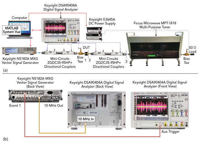
Figure 1 Measurement setup (a); auxiliary trigger and 10 MHz reference signal connections (b).
Custom MATLAB software controls the equipment and handles data acquisition via virtual instrument software architecture (VISA) commands. The voltage waveforms captured by the oscilloscope’s four channels are transferred to the computer, where they are processed to calculate the calibrated load reflection coefficients (ΓL) at the DUT’s output port, along with Pout, G, ηd, PAE and ACPR. A Keysight SystemVue schematic is employed to configure the VSG to generate the modulated signal required for the measurements.
Reflection Coefficient Measurement
ΓL is defined as the ratio of reflected to incident voltage at the output port. Its magnitude and phase are calculated separately to determine the uncorrected or raw ΓL from the acquired data. First, the time-domain waveforms of the incident and reflected voltages are analyzed to compute the phase. Since both signals share the same carrier frequency (see Figure 2), their phases are determined using zero crossings of the first period of each signal.24 The raw ΓL phase is then obtained by subtracting these values.
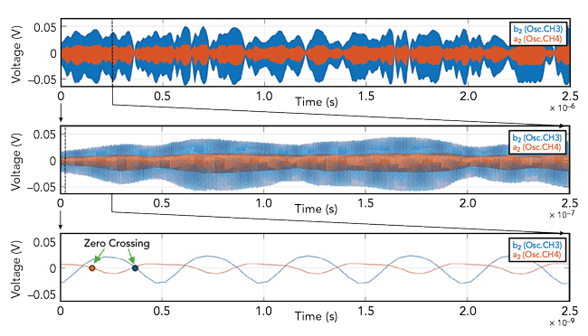
Figure 2 Example phase calculation of the modulated signal for voltages at the output port.
For improved accuracy, the oscilloscope’s averaging function is enabled during this process, enhancing the precision of the phase measurements and the subsequent calculation of the raw ΓL phase. The zero crossings are measured directly on the oscilloscope, then the oscilloscope’s averaging function is turned off before calculating the magnitude of ΓL. This is important because it has been observed that the oscilloscope’s averaging alters the amplitude of the signal when measuring a modulated waveform. This is most likely because the averaging function of most oscilloscopes is intended for repetitive signals, benefiting mostly periodic signals, and the modulated signal used for this test is not repetitive within the measured time lapse of 25 μs. At this stage, the voltage waveforms from all four oscilloscope channels are measured, captured and transferred to the computer for further processing.
The magnitude of ΓL is determined by computing the voltage’s fast Fourier transform (FFT). Since the measurements are performed using a modulated signal, the average power within the signal’s bandwidth for both the incident and reflected voltage spectra must be calculated. The magnitude of the raw ΓL is then obtained by taking the ratio of the reflected spectrum to the incident spectrum.
Power Measurements
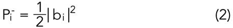
Conducting load-pull measurements requires determining the power at the DUT’s input and output ports. These calculations rely on fundamental principles and equations from transmission line theory.25 The incident (Pi+) and reflected (Pi-) powers are computed from the measured voltages using Equations 1 and 2:
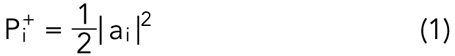
Where:
- i=1,2 corresponds to the input and output ports.
- ai and bi represent the normalized incident and reflected voltages at port i, calculated by dividing the measured voltages by √Z0, where Z0 denotes the characteristic impedance.
First, the FFT of the measured voltages is calculated. Then, the power of each spectral component within the signal’s bandwidth is determined using Equations 1 and 2. Finally, the total average power is computed by summing all the individual power spectral components.
Power measurements require calibration after determining the uncorrected incident and reflected average power at each port, as detailed in the following section. Once calibrated, the input power (Pin) and output power (Pout) are calculated using Equations 3 and 4:


Where P1+ and P1- refer to the incident and reflected power at the input port and P2+ and P2- correspond to the incident and reflected power at the output port.