

Efficiency Measurements
Drain efficiency (ηd) and PAE are calculated with Equations 5 and 6:
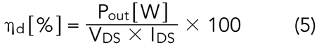
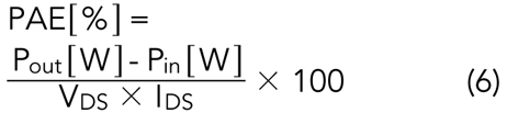
Where:
- VDS and IDS represent the bias drain-to-source voltage and the DC drain-to-source current of the transistor.
- Pin and Pout are the calibrated input and output power values.
ACPR Measurements
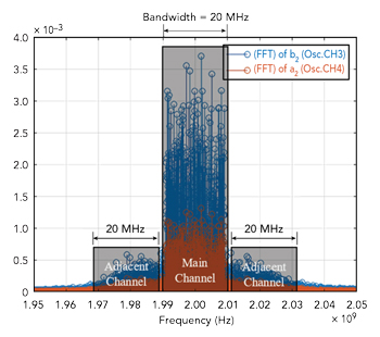
Figure 3 Magnitude of the FFT of voltages from Figure 2 indicating the bandwidths of the main and adjacent channels.
ACPR is the power ratio in adjacent channels to the power within the signal’s main channel. Figure 3 shows the FFT of the incident and reflected voltages in Figure 2, clearly illustrating the signal’s main and adjacent channels.
Measuring ACPR with this system requires calculating the power in the signal’s adjacent channels at the DUT’s output port. This process is like calculating Pout, with one key difference: the average incident and reflected power must be computed for the frequency range within the adjacent channels. The calculation is performed separately for the upper and lower adjacent channels, with a 1 MHz gap between the main channel and each corresponding adjacent channel.
After obtaining the incident and reflected average power for both adjacent channels, these values undergo the same calibration process as Pout. The adjacent channel power is then calculated using Equation 4.
CALIBRATION
Load-pull measurements involve multiple calibration steps before data collection, with specific procedures depending on the measurement setup. This work simplifies the calibration process, requiring only knowledge of the losses in the directional couplers and certain cables to calibrate power accurately.
Power Calibration
The first step is calibrating the power to deliver the desired power level to the DUT’s input port. This involves adjusting the VSG’s power level and correcting the measured power to compensate for any losses from the oscilloscope channels to the DUT’s ports.
This setup requires characterizing the losses of the directional couplers and cables from the oscilloscope channels to the DUT’s ports in advance. This is achieved using a power meter, spectrum analyzer or VNA. With these values, when a power measurement is taken, the losses must be accounted for by adding them to the measured power values. This enables the incident and reflected power to be determined at the DUT’s ports rather than at the oscilloscope channels.
Subsequently, Pin and Pout are computed using Equations 3 and 4. This simplifies the process by avoiding the more complex task of correcting the time-domain waveforms. Power calibration becomes more straightforward by focusing solely on power levels and losses in the setup.
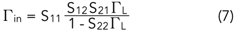
Since load-pull measurements involve varying ΓL presented to the DUT, the strong dependence of Γin on ΓL7,25 can cause the measured input power to deviate significantly from the expected value due to a highly reflective Γin at certain ΓL values. Consequently, when computing Pin using Equation 3, the measured Pin can be significantly smaller than expected. Although Γin was not explicitly computed, initial tests suggest that increases in reflected power affecting Pin match the theoretical dependence of Γin on ΓL, see Equation 7. So, in addition to the initial power calibration, an input power level adjustment sequence is implemented in the MATLAB code used for the measurements to resolve this issue.
The sequence involves measuring Pin and incrementally increasing the VSG’s output power level until Pin reaches the expected value. This adjustment is performed for each tuner position, ensuring that every measurement is conducted with a consistent input power level at the DUT’s input port, regardless of the DUT’s Γin.
Reflection Coefficient Calibration
The raw ΓL value is calibrated using the method outlined by Ferrero and Pisani,22 which involves performing open-short-load (OSL) calibrations at different reference planes within the measurement setup. The first OSL calibration is carried out at the reference plane labeled as 1 in Figure 1a. A thru standard is then connected at Reference Plane 1 to perform an OSL calibration at Reference Plane 2 that is used only during a validation step in the calibration process.
Then, after connecting the directional couplers between Planes 2 and 3, an OSL calibration is conducted at Reference Plane 3 before connecting the tuner. All reference planes are indicated in Figure 1a. This process provides the necessary values to compute the calibrated ΓL.
Finally, before starting the measurement, some ΓL values are measured with the thru still connected at the DUT’s ports to compare the measurement from the couplers at the input port (calibrated with the second OSL) with the measurements from the couplers at the output port (calibrated with equations from Ferrero and Pisani22). If the calibration is performed correctly, both ΓL values should be equal for each tuner position.
When all calibration measurements are completed, the DUT is connected in place of the thru standard, and the measurements proceed without any additional disconnections in the setup. Additionally, a thru-reflect-line (TRL) calibration26 is necessary to de-embed the effects of the transistor’s test fixture.
EXPERIMENTAL RESULTS
The signal used for the measurements is an LTE-modulated signal with an average power of 5 dBm, a center frequency of 2 GHz and a bandwidth of 20 MHz. An ATF38143 GaAs FET biased with VGS=-0.56 V and VDS=3 V is used. The results are shown in Figures 4 through 9, where the load-pull contours for Pout, G, ηd, PAE and both upper and lower ACPR are displayed on Smith charts generated using Focus Microwave’s Contour Viewer software.
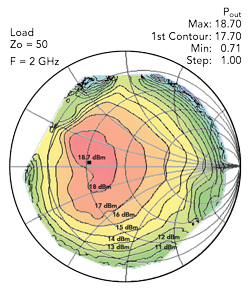
Figure 4 Measured output power load-pull contours.
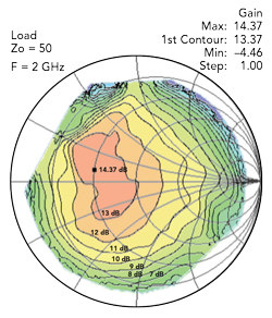
Figure 5 Measured gain load-pull contours.
These results offer a more accurate representation of the DUT’s performance when designing a PA intended to operate with modulated signals in its final application and provide the designer with the optimal ΓL values needed to achieve the desired performance.
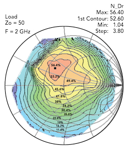
Figure 6 Measured drain efficiency load-pull contours.
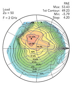
Figure 7 Measured PAE load-pull contours.
Analyzing the Pout and ACPR contours in Figures 4, 8 and 9 reveal that the ΓL values for maximum Pout are located on the Smith chart far from those that achieve the best performance for both the upper and lower ACPR. The same applies to the G, ηd and PAE contours, where their optimal ΓL values differ from those that provide the best ACPR performance. This information helps the designer choose the optimal ΓL to balance efficiency and linearity for an amplifier operating with a modulated signal, enabling analysis of the tradeoff between these factors based on a specific application.
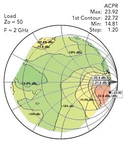
Figure 8 Measured upper ACPR load-pull contours. ACPR values are negative and expressed in dBc.
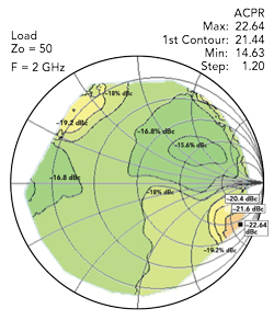
Figure 9 Measured lower ACPR load-pull contours. ACPR values are negative and expressed in dBc.
After performing the load-pull measurement, some ΓL values are selected to repeat the measurement using spectrum analyzers (SAs). The incident and reflected output power levels at both the main and adjacent channels are measured to validate all power-related calculations from the load-pull measurements.