

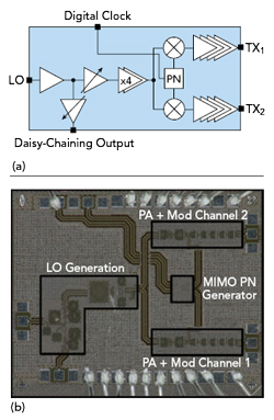
Figure 1 PMCW transmitter block diagram (a) and transmitter chip micrograph (b).
RF characterization up to D-Band (110 to 170 GHz) is increasingly necessary with the current drive toward 6G wireless communications, high speed digital links and advanced sensing technologies. Considering the sensing use case and the design and optimization of a D-Band power amplifier (PA), this article investigates the measurement challenges accompanying leading-edge RF technology development. The importance of measuring amplifiers with actual load conditions in an on-wafer test environment will be illustrated.
MMWAVE SINGLE-CONNECT IS THE NEW NORMAL
In 1950, Rohde & Schwarz achieved a remarkable milestone: creating the first vector network analyzer (VNA). This instrument characterized single-port S-parameters to 300 MHz, a breakthrough in RF measurements. Seventy-five years of technological development later, RF design and testing have evolved to where mmWave characterization is the new normal. A single measurement setup captures more than S-parameters and provides a complete performance overview of the device under test (DUT) after one calibration and connection.
Single-touchdown is of the utmost relevance to IC design where costly and fragile die are measured with delicate probing systems. RF components and modules, typically made for matching 50 Ω conditions, are now used in complex, non-ideal environments. It is a common requirement for semiconductor foundries to provide 50 Ω reference specifications and accurate models to enable system integrators and IC designers to achieve the best system performance.
This article discusses challenges in large-signal characterization of D-Band PAs using a sub-THz load-tuning measurement setup.
D-BAND AMPLIFIER FOR SENSING APPLICATIONS
Large channel bandwidths in D-Band create new possibilities for high-resolution imaging, radar and high data-rate communication systems. PAs are a key building block in these applications and are used before transmit chain antennas or as a driver stage for a frequency multiplier or mixer. Advanced silicon-on-insulator (SOI) CMOS technologies achieving an ƒT and ƒmax of 350 GHz and 370 GHz, respectively, are suitable for low-power, high efficiency mmWave circuits. Despite the high performance of mmWave transistors, achieving high output power at D-Band frequencies is still challenging. The short gate length, which results in low operational and breakdown voltages, is a critical output power limiting factor.
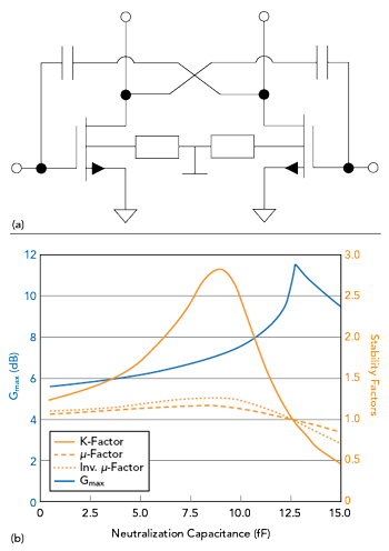
Figure 2 Pseudo-differential topology (a) and 140 GHz performance (b).
Using transistors with longer gate widths and higher current swings can increase output power. However, this creates a significant gain reduction at high frequencies, caused mainly by increased parasitic gate-drain and gate-source capacitance. Enlarging the transistor gate width also decreases the optimum output impedance. The transformation ratio to 50 Ω becomes larger and may lead to lossier matching networks. Power-combining is a common approach to increase output power.
However, this requires additional complex dividers and combining structures, increasing loss, DC power and chip area.1,2 SOI technology enables transistor stacking to increase the maximum voltage swing, which has already been successfully demonstrated at lower frequencies.3 Nevertheless, this amplifier topology requires an increased nominal supply voltage, which can require special care and have disadvantages for integration into larger systems.
Two implementations of compact, energy-saving and high efficiency D-Band PAs have been proposed.4 These PAs operate at 0.8 V supply voltage on 22 nm fully-depleted SOI (FD-SOI) technology. The PAs are part of a gesture/motion recognition in a phase-modulated continuous wave (PMCW) radar transceiver system. This emerging application allows new man-machine interfaces and supports non-invasive vital sign assessment. The radar architecture was introduced by F. Probst et al.5 Figure 1 shows the Tx architecture and a micrograph of the chip and the relevant building blocks. Two broadband transmit antennas and the Tx chip are integrated into an embedded wafer-level ball grid array (eWLB) package.
The antenna/Tx interconnection has significant losses at D-Band frequencies. Chip placement and subsequent processing of the antenna redistribution layers are highly dependent on process tolerances, creating modeling and interconnection challenges. The PA design ensures sufficient output power to the antennas, even when manufacturing tolerances change antenna input impedances. Load sensitivity simulations and measurements are necessary to evaluate this essential capability of the PA.
The amplifier stages employ a pseudo-differential topology. Figure 2 shows the differential common-source transistor pair schematic with cross-coupled neutralization capacitors (CN). These capacitors boost gain and increase differential mode stability by compensating for the parasitic gate-drain capacitance (Cgd). CN overcompensates Cgd, resulting in a three to four dB gain increase instead of maximizing stability. Figure 2 shows the CN influence on the maximum available gain (Gmax), K and μ stability factors at 140 GHz. To limit compensation network losses, CN are alternated polarity metal-oxide-metal (APMOM) capacitors. The back-gate bias voltage feeds two resistors, RBG and aids operation point tuning.
Each PA has three drivers for sufficient gain and one high-power output stage. Figure 3 shows a simplified block diagram of the two PAs. Tuning the driver gain to slightly different frequencies enhances amplifier bandwidth, while load-pull simulations optimize the output-matching network to maximize the available output power. Each stage uses super-low threshold voltage (SLVT) n-MOS transistors with double gate-pitch, double-sided gate connection and minimum channel length of 20 nm. Two parallel, 600 nm finger-width transistors are used as driver stages to account for the gate resistance/parasitic finger capacitance trade-off. Three parallel 800 nm finger-width transistors comprise the output stages. Output PA stages are biased for class AB operation for better efficiency, while the drivers are biased in class A for high gain. Two mmWave implementation methods were investigated for the input, output and interstage matching networks. The first uses stacked transformer-based (TB) matching, while the second uses T-line-based (LB) networks.
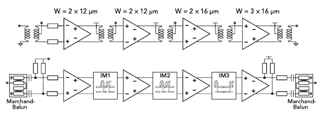
Figure 3 TB-PA (top) and LB-PA (bottom).
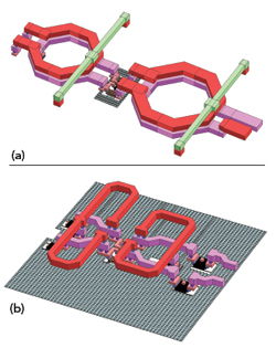
Figure 4 Input- and output-matching networks of the TB-PA (a) and LB-PA (b).
Figure 4 shows 3D views of the TB-PA and LB-PA output stages. The TB-PA benefits from the transformer’s compact device size and the ease of routing the DC feed over the center tabs. Short T-lines between the input transformer and the first PA stage provide more efficient impedance matching. For measurement purposes, input and output transformers are baluns. The main drawback of this design is the increased effort to generate accurate circuit models encompassing all relevant D-Band parasitic effects.
The LB-PA implementation benefits from less complex T-line device modeling and more straightforward modular design flows. Taking advantage of the differential circuit’s symmetry and the two available thick copper layers, the shorted T-line stubs can be rolled up, as shown in Figure 4. This layout results in a compact design and the LB matching network dimensions are comparable to the TB realization. The symmetry points provide good DC bias and supply voltage feed connections. Additional capacitors are inserted between stages to separate gate bias and supply voltage feeds, resulting in additional matching network losses. Another drawback is the necessity of auxiliary components for single-ended-to-differential conversion required for on-wafer measurements. This requires broadband Marchand baluns at the LB-PA input and output, resulting in extra chip area and increasing fabrication cost.
Load-pull simulations determine the optimal PA matching impedance. Figure 5 shows the 140 GHz load-pull simulation results for the TB-PA output stage. The maximum achievable output power of the stage at the optimal load point, Zopt, is 8.7 dBm. The output impedance, Zout, of the PA stage and the input impedance of the matching balun, Zm, are displayed over frequency with a 140 GHz marker. The matching balun brings the 50 Ω load close to the optimum load point but introduces approximately 1.8 dB loss, reducing the maximum achievable output power.
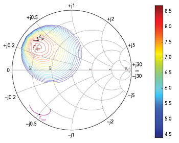
Figure 5 Simulated 140 GHz load-pull power contours.
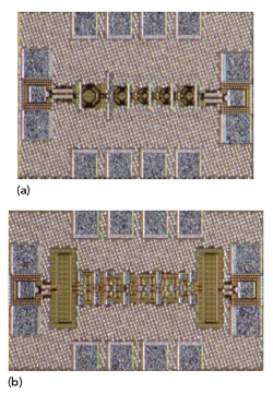
Figure 6 TB-PA (a) and LB-PA (b) micrographs.
Figure 6 shows the chip micrographs. The total areas, including pads and baluns, are 0.326 mm2 (TB) and 0.34 mm2 (LB).