

BUILDING THE COMPLETE ON-WAFER MEASUREMENT SYSTEM
The core instrument for RF PA validation is often a VNA. This one-box instrument offers many measurement capabilities that are needed to characterize and optimize a PA. The baseline S-parameters enable the derivation of device parameters like gain, gain compression, amplitude and phase distortion. Pulsed S-parameters, harmonic measurements, noise figure and intermodulation points are additional KPIs that come from an enhanced VNA with an extended feature set. If the DUT is not adequately cooled, pulsed S-parameter measurements may avoid overheating.
PAs are often used beyond their linear range to enhance power efficiency. Here, traditional small-signal S-parameters are not valid. However, a VNA can still determine the corresponding wave quantities, as shown in Figure 7.
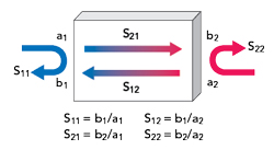
Figure 7 Definition of a and b wave quantities.
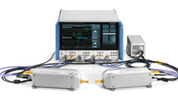
Figure 8 ZNA VNA with mmWave converters.
External frequency converters commonly extend VNA measurements into sub-THz frequency ranges, reaching 1.1 THz and beyond. The VNA controls the converters and the VNA user interface shows the target frequencies. Figure 8 shows a VNA with external converters. External converters placed near the DUT minimize losses.
LOAD-PULL
Different impedances are presented to the DUT input/output for comprehensive device characterization and optimization. This replicates the effect of dispersive loads, as an antenna might create. It also unveils the DUT optimization potential and the matching circuitry that optimizes gain, efficiency and other KPIs. This is important since devices behave differently under various impedances. The unpredictable behavior across different conditions requires extensive measurements to create and optimize accurate simulation models. By controlling independent parameters, the load-pull procedure allows DUT performance mapping under different impedances. The optimal performance condition can be established by plotting the DUT performance.
A common approach for creating different impedances is passive load-pull, which uses mechanical tuners to create a varying load. This approach is scalable in frequency and applicable up to 330 GHz. Figure 9 displays a passive load-pull system block diagram.
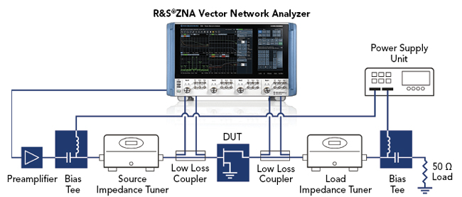
Figure 9 Typical passive load-pull setup.
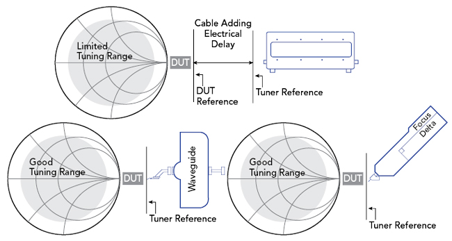
Figure 10 Conventional tuner structure versus Focus Delta tuner with direct RF probe connection.
Figure 11 R&S ZRX170L mmWave mini receiver modules.
Impedance tuners generate a reflection factor that can be controlled over a defined frequency range using the mechanical movement of complex loads within the tuner. In passive load tuning, the returning signal, a2, is always smaller than the transmitted signal, b2, because of transmission losses and tuner reflection. Therefore, the magnitude of the reflection coefficient, Γ, is always < 1 and the impedance point resides inside the Smith chart. The outer range of the Smith chart is not reachable in a pure passive load-pull system. Reducing loss in the tuner and transmission line between the DUT and the tuner enables a larger accessible Smith chart range, as shown in Figure 10.
Adding frequency converters to D-Band frequencies adds complexity to the setup. To optimize the dynamic range for the receive channels of the forward and reverse waves, a and b, the tuner separates these signals on the input and output sides of the DUT. Specific down-converter receivers, shown in Figure 11, measure the independent signals.
Measuring the a and b waves allows the vector load-pull to calculate the real-time tuner impedances presented to the DUT. A standard converter on the DUT’s input side provides the test signal. Figure 12 shows the RF and IF signal flow, along with the measurement and calibration components. A second converter and power sensor are added for calibration.

Figure 12 Frequency-converted load-pull system.
COMPLETE ON-WAFER SETUP
The setup uses a probe station to contact the DUT shown in Figure 6. The challenge is to combine DC and RF probing efficiently. Precaution was taken to have similar landing pads between the two PA variants. Pads often have a combination of DC, digital and RF channels. Based on the layout, one probe needs to support the different channel functions. The MPI TITAN™ Multi-Contact Probe, which supports mixed-signal characterization requirements, shown in Figure 13, handles high-density probing needs, covering pitches down to 50 μm.
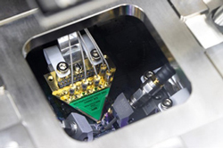
Figure 13 Multi-contact probe solution.
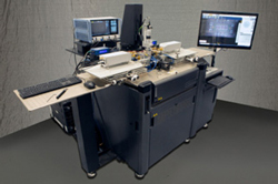
Figure 14 On-wafer characterization system.
As discussed, precise probe positioning is essential to minimize loss between the tuner and DUT. Direct probe connection to the tuner eliminates additional transitions. A waveguide transition is typical in this frequency range to minimize loss while providing a stable connection without phase drift. This transition between the tuner and the mmWave receiver modules or the mmWave converter requires precise positioning. The probe station must support this to enable room for additional amplification blocks or isolators. To address mechanical constraints for this complex setup, MPI Corporation developed a four-axis positioner to support the D-Band tuner plus the measurement system components. The RF connections are on opposite sides of this configuration, while the DC/mixed-signal probes occupy the other opposite sides. MPI’s large-area MP4X positioners provide support for the rigid waveguide setup, ensuring mechanical stability and minimizing phase drift during D-Band measurements for repeatable and accurate testing. Figure 14 shows the test system. The screen offers an enlarged view of the DUT from the installed microscope. Figure 15 shows a close-up of the DUT, probes, blue tuners, mmWave receivers and the converters on the sides.
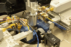
Figure 15 Close-up of the on-wafer system.
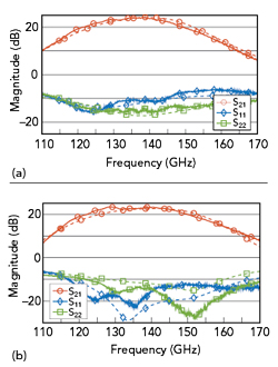
Figure 16 Simulated (dashed) and measured (solid) S-parameters without load pull: TB-PA (a) and LB-PA (b).