

SYSTEM-LEVEL CALIBRATION AND CONTROL
System calibration is important for VNA measurements. There are two steps:
- Calibrate the on-wafer system with the VNA and its converters using MPI calibration solutions and the accompanying software, including test coupons as calibration standards
- Calibrate the system load-pull tuners with the Focus Microwaves software.
Once calibration is complete, the Focus Microwaves software acts as the system software. It controls the applied impedance using the tuners and the R&S ZNA to perform the RF measurements for device characterization. The MPI prober ensures stable test conditions in positioning: a cold plate and a controlled, integrated airflow within the probe station cool the DUT.
D-BAND PA MEASUREMENTS
Engelmann et al.4 reported validation results for two PAs without load-pull. Figure 16 shows this comparison and S-parameters for TB-PA and LB-PA (including balun and pad losses). Peak small-signal gains of 24.2 and 23.4 dB with 3 dB bandwidths of 23 and 26.2 GHz around the center frequencies of 135.3 and 135.8 GHz were achieved for TB-PA and LB-PA. Both PAs have reverse isolation, S12, < -37 dB over the D-Band frequency range.
Figure 17 shows large-signal measurements without load-pull. It shows more significant deviations in saturated output and PAE, particularly for the TB-PA architecture. The PA saturation region deviation is hard to explain when analyzing only small-signal S-parameters since large-signal effects cannot be considered accurately.
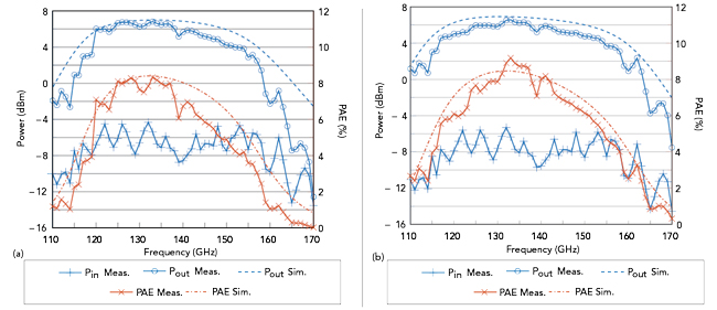
Figure 17 Simulated (dashed) and measured (solid) Pout and PAE without load pull: TB-PA (a) and LB-PA (b).
As expected, the LB-PA is relatively insensitive to the load impedance, thanks to its output-matching network and broadband Marchand baluns. Figure 18 illustrates the LB-PA Pout distribution as a function of the load in linear, 1 dB compression and saturated regimes.
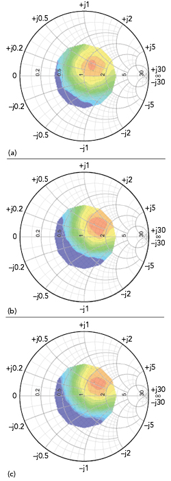
Figure 18 LB-PA load-sensitivity measurements: (a) small signal; (b) 1 dB compression and (c) saturated.
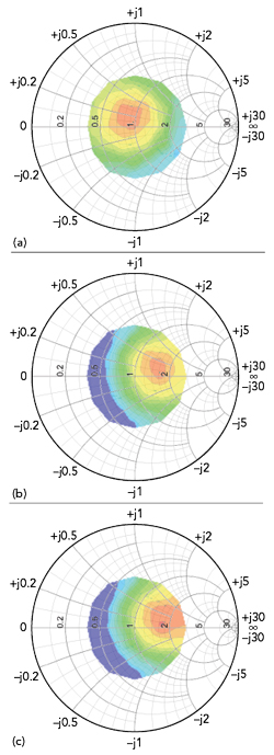
Figure 19 TB-PA load-sensitivity measurements: (a) small-signal Pout; (b) saturated Pout and (c) saturated PAE.
As expected, the TB-PA load-pull measurement shows more sensitivity to load variations in Figure 19. The output power contours shift drastically from the small-signal to the saturation region. The maximum small-signal output power occurs near the Smith chart’s center, indicating excellent 50 Ω small-signal matching. This, however, changes with increasing output power, shown by the constant power contour shift to higher impedances. Output-matching network model inaccuracies, especially at higher frequencies, are the likely cause of the 50 Ω load not transforming to the optimum load point, Zopt, for maximum achievable power. Deviations in the load-pull simulations used to determine Zopt are another possibility. However, LB-PA should show similar deviations. The measurement results provide enhanced insights into the PA’s large-signal behavior, which simplifies understanding the simulation-to-measurement deviations. The load-pull measurement enables better device modeling and indicates PA load sensitivity. For the PMCW PA Tx module in Figure 2, load-pull data validates whether the impedance variations of the antenna will degrade the PA output power and the overall system performance.
CONCLUSION
This article addressed the complexity of RF characterization at mmWave and sub-THz frequencies and provided an example of on-wafer D-Band amplifier measurements. Two specific PAs designed for radar sensing applications were investigated using different architectures and output-matching approaches. The example stresses the importance of accounting for load-pull when characterizing active components in the mmWave and sub-THz frequencies, particularly when looking at large-signal parameters.
Acknowledgments
The authors would like to thank Dr. Sajjad Ahmed at Focus Microwaves and Vince Mallette at MPI Corporation for their excellent collaboration and support for the on-wafer load-pull test system. The authors want to express their gratitude to GlobalFoundries for providing silicon fabrication through the 22FDX® university program. The PA design work was initially funded and supported by the Federal Ministry of Education and Research (BMBF), Germany, through the joint research project REGGAE within the ForMikro research initiative under grant 16E106S1.
References
- 1. D. Simic and P. Reynaert, “A 14.8 dBm 20.3 dB Power Amplifier for D-band Applications in 40 nm CMOS,” IEEE Radio Frequency Integrated Circuits Symposium (RFIC), 2018, pp. 232–235.
- 2. J. Zhang, T. Wu, L. Nie et al., “A 120–150 GHz Power Amplifier in 28-nm CMOS Achieving 21.9-dB Gain and 11.8-dBm Psat for Sub-THz Imaging System,” IEEE Access, Vol. 9, 2021, pp. 74 752–74 762.
- 3. M. Cui, Z. Tibenszky, D. Fritsche et al., “An Area Efficient 48 - 62 GHz Stacked Power Amplifier in 22nm FD-SOI,” 14th European Microwave Integrated Circuits Conference (EuMIC), 2019, pp. 120–123.
- 4. A. Engelmann, P. Hetterle, F. Probst, R. Weigel and M. Dietz,” Design of Two Low DC- Power High-Efficiency D-Band Power Amplifiers in 22 nm FDSOI,” 17th European Microwave Integrated Circuits Conference (EuMIC), Milan, Italy, 2022, pp. 212–215, doi: 10.23919/EuMIC54520.2022.9923463.
- 5. F. Probst, A. Engelmann, M. Koch and R. Weigel,” A Dual-Channel 15 Gb/s PRBS Generator for a D-Band PMCW Radar Transmitter in 22 nm FDSOI,” IEEE Wireless and Microwave Technology Conference (WAMICON), 2023, pp. 129–132, doi: 10.1109/WAMICON57636.2023.10124888.