
With advancements in system integration and high speed data converters, high performance phased array antenna (PAA) systems become practical in very small form factors. This expands their use cases in a variety of communication and RF sensing applications.1,2 This article discusses the performance characterization challenges associated with highly integrated RF front-end and digital baseband devices, including the RF path in digital beamforming or software-defined radio devices, RF transceiver ICs and high speed data converters. The development of a new digital and RF cross-domain stimulus/response method is introduced using a vector network analyzer (VNA) and measurement examples are provided for a digital and RF mixed signal device.
Typical communication and RF sensing systems are configured with RF front ends, frequency up- and down-converters and digital baseband sub-modules with signal conditioning in each stage, as required. When RF systems are used on various platforms, such as unmanned aerial vehicles, airplanes (conformally mounted to the surface) or mobile equipment—size, weight and power consumption must be considered for platform compatibility. As more versatile and capable RF systems are developed for small platforms, the level of integration continues to accelerate.
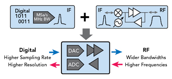
Figure 1 New RF front-end architecture with integrated high speed data converters.
Highly integrated RF systems often consist of multiple RF channels, minimized interconnects between functional blocks, the possible introduction of direct RF to digital conversion and the migration of hardware functions to software signal conditioning and analysis (see Figure 1). This new RF front-end architecture becomes practical with advancements in higher frequency packaging and high speed data converters, i.e., analog-to-digital (ADC) and digital-to-analog (DAC). Such integrated RF front-end architectures bring many benefits such as improved performance, wider operating frequency ranges and greater flexibility. They also introduce many new challenges, however, especially for design verification and testing.
RF PERFORMANCE CHARACTERIZATION CHALLENGES
Engineers are well equipped with test instruments for performance characterization on RF systems under development if the device under test (DUT) is defined with RF input and output ports. Unfortunately, this is no longer the case for highly integrated RF systems. The DUTs are defined with mixed RF and digital input and output ports, such as digital baseband integrated RF front ends, wideband transceiver ICs and high speed data converters.
Digital Data Analysis
Modern digital and RF integrated devices and modules contain high speed data converters, often capable of giga-samples per second sample rates. Testing the front-end RF performance of these devices requires recording and analyzing the digital output data bits. As the sampling rate increases for greater bandwidth, more digital data must be processed and analyzed. Recording digital data to analyze the entire operating RF band becomes time consuming. For systems with many RF paths such as PAA systems, this must be repeated hundreds of times, making complete characterization time consuming and costly.
Conventional Test Tool Limitations
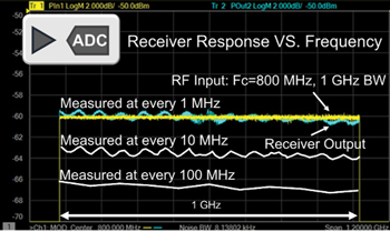
Figure 2 Receiver frequency response vs. frequency resolution.
VNAs are commonly used for precise performance characterization of RF front-end modules and components. However, the RF stimulus response measurement and calibration methodologies used in VNAs are no longer suitable for testing devices that directly convert digital and RF signals. Therefore, RF signal analyzers and generators are the only available options. The drawback is that the measurements often rely on assumptions of linearity and signal fidelity of the instrumentation used and the digital data analysis capability of the engineers. This makes current measurement options not nearly as dependable as the VNA’s RF stimulus response methodology.
Performance Deviation in Higher Frequencies and Wider Bandwidths
The operating frequencies of RF systems with high speed data converters continue to increase, sometimes up to mmWave frequency ranges. The end applications use designated frequency channels in these frequencies, but the equipment needs to be tested over the entire operating bandwidth. As RF performance becomes frequency dependent at higher frequencies and wider bandwidths, it is important to test at finer frequency resolutions to obtain an accurate understanding of frequency dependencies (see Figure 2). It is simple for RF devices that can be characterized with traditional VNA measurement techniques. However, it becomes more difficult and requires more effort for digital and RF mixed signal devices.
DIGITAL RF CROSS-DOMAIN STIMULUS AND RESPONSE MEASUREMENT METHOD
This new test methodology addresses the engineering challenges in digital and RF mixed device performance characterization. It is based on the well-known RF stimulus response methodology used in traditional VNA measurement techniques, but is modified to accommodate digital waveforms for either stimulus or response.
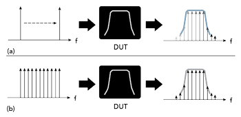
Figure 3 Swept single tone stimulus response (a) vs. wideband multi-tone stimulus response (b) methods.
An ordinary VNA’s stimulus response measurement methodology uses a swept single tone stimulus with a tuned narrowband receiver for frequency response measurements. In contrast, the new approach includes a wideband multi-tone stimulus capability with a wideband analysis technique to yield the device’s frequency response (see Figure 3).3 The test waveform (digital or RF) is precisely defined and repeatedly played for the response wave (digital or RF) and can be coherently correlated at each spectral component with the stimulus waveform, resulting in vector response measurements between input and output signals within the stimulus waveform bandwidth.