
This new cross-domain stimulus response methodology yields RF performance characteristics of digital and RF mixed devices over frequency or power ranges in one set of measurements, while it takes days or weeks for the same measurements using the traditional approach—stimulating with a single tone at a fixed frequency and capturing the response at a single frequency point.
MEASUREMENT EXAMPLES
Measurement System Configuration
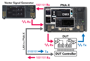
Figure 4 Wideband transceiver IC measurement setup.
The measurement system configuration is shown in Figure 4. The DUT used in the measurement examples is a commercially available wideband RF transceiver IC mounted in its manufacturer’s evaluation kit with an integrated DUT controller. It includes multi-channel transmitters and receivers with 12 GSa/s DACs and 6 GSa/s ADCs, respectively. The measurements are completed with one transmitter and one receiver channel. The application software called Device Measurement Expert (DMX) with cross-domain test capability controls the N524xB PNA-X VNA and the external vector signal generator (VSG).
When testing receivers, the DMX defines the digital IQ waveform for the VSG to generate, which is measured with the PNX-X’s reference receiver in addition to the receiver under test. The DMX uploads the digital IQ waveform file generated from the receiver and the VNA processes the data. When testing transmitters, the DMX sends the digital IQ waveform to the transmitter under test and the PNA-X’s reference receiver. The PNA-X measures the output RF waveform from the transmitter and processes the data. This configuration enables receiver, transmitter and transceiver measurements with a single set of connections.
Calibration
Measurement system calibration on the VNA is available on this setup, limited to the RF test ports. When measuring transmitters, the stimulus is digital and treated as an ideal waveform and the RF response waveform is measured with the calibrated test receiver of the VNA. When measuring receivers, the stimulus is an RF waveform that is distortion-corrected and measured using the VNA’s calibrated reference receiver. The digital response waveform is then measured by the receiver under test. In the RF stimulus waveform correction process, the waveform is pre-distorted to account for the source distortion errors in addition to linear errors. This results in an RF stimulus that is a nearly ideal waveform at the receiver input. The effect of source distortion correction is reviewed in the following section.
Frequency Response Measurements
The measurement example in Figure 5 demonstrate fast receiver and transmitter gain flatness versus frequency measurements. It includes nearly one thousand frequency response points on each measurement, with 1.1 MHz resolution in a 1 GHz bandwidth at 4 GHz center frequency in the receiver measurements (see Figure 5a), and with 2.2 MHz frequency resolution in a 2 GHz bandwidth at 4 GHz center frequency in the transmitter measurements (see Figure 5b).
The measurements were completed in only a few minutes including time for device initialization using the new measurement methodology described previously. This is a remarkably short time compared to the traditional method of point-by-point measurements obtained from single tone measurements using a signal generator and a signal analyzer.
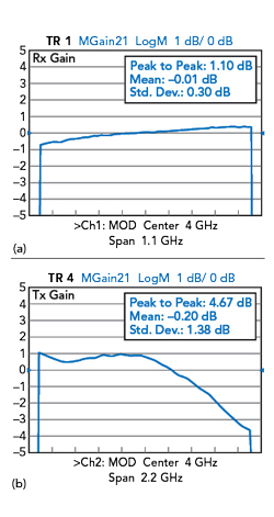
Figure 5 Measured gain flatness: 1.1 dB for the receiver (a) and 4.67 dB for the transmitter (b).
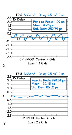
Figure 6 Measured deviation from average delay: 1.09 ns for the receiver (a) and 320.5 ps for the transmitter (b).
The same measurement setup yields deviation of average delay measurements across the entire operating bandwidth with no additional effort (see Figure 6). With the repetitive multi-tone stimulus response method, phase responses are effectively stitched between repeated measurements, resulting in virtually unlimited analysis bandwidth.
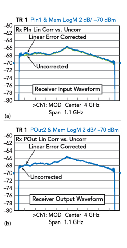
Figure 7 Effect of linear error correction: receiver input (a) and output (b) waveforms
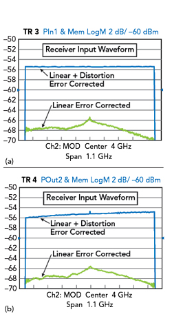
Figure 8 Source distortion may significantly affect receiver response measurements: receiver input waveform (a) and output waveform (b).
Corrected Versus Uncorrected Measurements
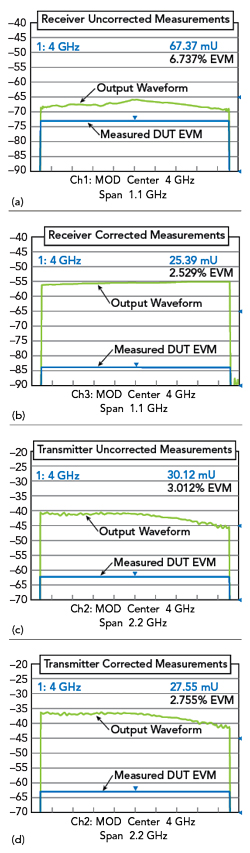
Figure 9 EVM measurements: receiver uncorrected (a) and corrected (b); transmitter uncorrected (c) and corrected (d).
These receiver measurements highlight the impacts with available error correction options (see Figure 7). The first compares uncorrected and linear error corrected measurements with an input waveform (see Figure 7a) and measured with the VNA’s reference receiver (see Figure 7b). The output waveform is measured with the receiver under test. The effect appears as a slight adjustment. If there were more test accessories in the path between the test instruments and the receiver’s input port, such as longer test port cables and switch matrices, the linear errors would be more noticeable.
The next series of measurements only compares measurements between linear error correction, and linear and source distortion error corrections (see Figure 8). The RF receiver input waveform level is adjusted by nearly 6 dB to nearly an ideal flat-level input stimulus across a 1 GHz frequency bandwidth, which is expected to influence the receiver response. The corresponding output waveform exhibits the receiver’s frequency dependency clearer than results with source distortion uncorrected stimulus.
Error Vector Magnitude (EVM) Measurements
The new measurement methodology also allows distortion measurements of digital RF mixed devices.4 The examples shown in Figure 9 include corrected and uncorrected receiver and transmitter EVM measurements. Error correction in receiver measurements includes both linear error and source distortion corrections. There is noticeable EVM improvement in receiver measurements and the source-generated distortion is minimized for accurate receiver performance characterization. Linear error corrections are only applied in the transmitter test because the RF source is the DUT. The signal distortion introduced by the RF source in the transmitter is what is of interest to be characterized.
CONCLUSION
The new digital RF cross-domain stimulus response methodology demonstrates fast and precise digital and RF mixed signal device characterization. This approach leverages commonly used RF test instruments like VNAs and VSGs for testing new types of digital RF mixed devices, which are expected to be common building blocks of RF front-end architectures in the foreseeable future. Existing error corrections are helpful for improved measurement accuracy, although some residual errors still need mitigation techniques such as undesired-signal isolation. EVM measurements, in addition to frequency response measurements, are useful as these RF systems become integrated into communication applications.
Future RF systems with mixed digital and RF architectures will continue to grow with broad applications. More measurement capabilities are expected to become available to meet the diverse end-application requirements. This includes not only linear response, but also noise and distortion performance characteristics.
ACKNOWLEDGMENT
The authors would like to thank the Analog Devices technical support team, Keysight VNA FW team and many Keysight scientists for technical assistance and feature implementation to realize this new measurement methodology.
References
- C. F. Castillo-Rubio and J. M. Pascual, “Current Full Digital Phased-Array Radar Developments for Naval Applications,” IEEE International Symposium on Phased Array Systems and Technology, October 2019.
- P. Delos and M. Jones, “Digital Array Using Commercial Transceivers: Noise, Spurious, and Linearity Measurements,” IEEE International Symposium on Phased Array Systems and Technology, October 2019.
- J. P. Teyssier, J. Dunsmore, J. Verspecht and J Kerr, “Coherent Multi-Tone Stimulus-Response Measurements with a VNA,” 89th ARFTG Microwave Measurement Conference, June 2017.
- J. Verspecht, A. Stav, J.P. Teyssier and S. Kusano, “Characterizing Amplifier Modulation Distortion Using a Vector Network Analyzer,” 93th ARFTG Microwave Measurement Conference, June 2019.