
Over the last several years, III-V heterojunction bipolar transistors (HBT) have become an increasingly important technology for a variety of rapidly growing markets. GaAs-based HBTs now play a major role in wireless communications. Key applications include power amplifiers for handset phones, wireless LAN and numerous other high speed analog circuit applications. Somewhat more recently, ultra high speed InP-based HBTs are being recognized as an attractive new technology for high data rate communication applications.
III-V HBTs have unique properties that confer important advantages compared with standard Si-based homojunction bipolar junction transistors (BJT). In particular, bandgap engineering in the emitter-base junction generally enables III-V HBTs to have a higher fT breakdown product than Si BJTs, allowing higher speed for the same breakdown voltage or more power at higher speeds. This advantage of III-V material systems persists even when compared to SiGe HBTs, which have recently produced impressive speed numbers, but cannot match the power of GaAs HBTs. Therefore, GaAs and InP-based HBTs are increasingly important to critical areas of growing technology markets.
In order to develop products based on these new technologies, it is necessary to have reliable design software with accurate models. In particular, it is critically important to have accurate large-signal models of the HBT devices, which are at the core of the technology. Accurate models reduce the number of design iterations in the product development cycle. Moreover, accurate nonlinear models can provide further insight into the workings of the device and the semiconductor process in which it is manufactured.
Unfortunately, most models used for simulating HBTs in commercially available simulators have significant shortcomings. Many of these problems stem from trying to represent the behavior of III-V HBT devices with models originally developed for Si BJT technology. Si-based BJT models, such as the venerable Gummel-Poon model, VBIC model, and even advanced models such as MEXTRAM and HICUM models, cannot naturally fit the detailed bias-dependence of GaAs- and InP-based devices well, and therefore struggle to predict distortion in applications using III-V technology.
AgilentHBT Model
This article presents the AgilentHBT model, a newly available nonlinear circuit simulation model designed explicitly for III-V (GaAs and InP) HBTs. The model was originally developed by the Agilent Technologies' Worldwide Process and Technology Center in Santa Rosa, CA for Agilent-internal III-V HBT semiconductor process development and high performance HBT ICs for broadband RF/microwave/millimeter-wave instrumentation.1 The model has been extracted and extensively validated in many real world conditions at the device and circuit levels, using devices from many different HBT semiconductor processes both within and outside Agilent.
The AgilentHBT model leverages the essential compound semiconductor physics-based model introduced in the DARPA/UCSD HBT model, widely referred to as the "UCSD model."2,3 Significant advances and improvements over this model, as well as a robust implementation in ADS, have been achieved. This makes the AgilentHBT a preferred alternative to Si-based BJT models or university written code for serious and accurate product design in III-V HBT technology.

A major innovation of the AgilentHBT model is its comprehensive nonlinear transit-time model. The inverse transit time is related to the fundamental velocity-field characteristics of charge carriers in the particular semiconductor material in which the device is fabricated. The velocity-field characteristics of III-V semiconductors are qualitatively very different from Si-based semiconductors, as shown in Figure 1. The high peak carrier velocity is an important advantage of the III-V devices. As can be observed from the figure, the change of carrier velocity with field (after the peak) in III-V material is opposite that of silicon. This difference is reflected at the device level where III-V transistors have the opposite voltage dependence of fT - a device-level measure of speed - compared with Si-based transistors.
The AgilentHBT model incorporates the current and voltage dependence of capacitances and transit times into a mathematically consistent charge-based formulation. It fundamentally resolves an inconsistency in the formulation of the UCSD model. The AgilentHBT model is both more accurate and flexible than the UCSD model. The AgilentHBT model can accurately fit the current and bias dependent behavior of the fT of devices from both GaAs and InP material systems, for widely varying device epitaxial designs, over a wide region of operating conditions (voltage and current). The ability to fit fT versus current and voltage is a requirement to accurately simulate low level distortion products, as demonstrated in the literature.4 Proof of this capability is presented in the Example Simulation Results section.

The AgilentHBT model equations have been implemented to insure a high degree of continuity required for both accurate distortion and good convergence properties. This represents an improvement in implementation over the prototype reported in Iwamoto, et al.1 Constitutive relations (I-V and Q-V relations) are infinitely differentiable and valid for all values of voltages. Accurate small-signal model equivalent circuit elements are derived from the large-signal equations, and can be reported by ADS at any user-specified operating point. This detailed information (see Figure 2 ), which includes figures of merit such as fT and gm , provides the designer with an intuitive understanding of the device operating conditions. A selection of key model features and their corresponding benefits are summarized in Table 1 .
|
TABLE I | |
|
Key Features | Benefits |
|
Charge-based nonlinear collector transit time formulation which models |
Accurate fit to III-V device characteristics, such as fT (VBC , IC ) and CBC (VBC ,IC ) which are critical to simulating distortion |
|
Empirical DC model for high current saturation effects |
Accurate fit to "soft-knee" for both single and double HBTs |
|
Infinitely differentiable and everywhere defined equations |
Necessary for accurate distortion and robust convergence |
|
Detailed device information including small-signal equivalent circuit element values from linearized equations |
Quantitative information to designers on device characteristics in the circuit language they often prefer |
|
Temperature dependent electrical |
Accurate simulations at different ambient temperatures |
|
Noise model including 1/f, burst |
Accurate phase noise and other nonlinear noise simulations |
Example Simulation Results
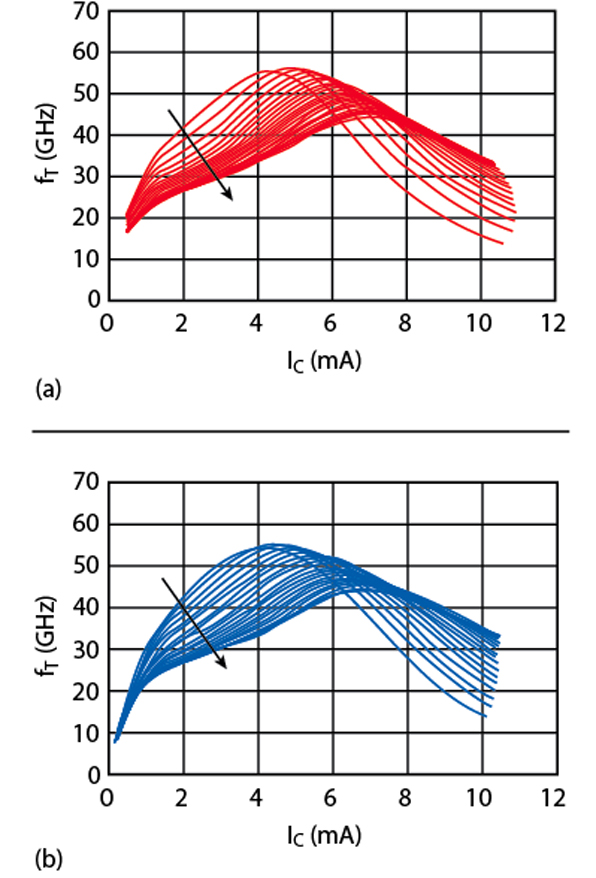
One of the significant features of the AgilentHBT model is the accurate transit time (delay) formulation, which has a direct impact on the fT behavior of the device. Figure 3 shows measured and simulated fT vs. IC curves presented over a very wide range of currents of voltages. This particular InGaP/GaAs HBT has a breakdown voltage (BVceo ) of 14 V, which is a typical device used in power amplifiers for wireless communications. The shape of the measured bias dependent fT behavior is very complex and the model is capable of reproducing the subtle details over a wide range of operating conditions. This is a critical capability of the nonlinear model because the magnitude and derivatives of the fT curves have a direct impact on the device distortion behavior. For example, Figure 4 shows measured and simulated third-order intermodulation (IM3) products versus current at various values of collector voltages. With close inspection, it is evident that the IM3 vs. Ic curve at a fixed voltage is intimately related to the fT vs. IC behavior. For example, the maximum in IM3 occurs near the fT peaks versus current, that is consistent with published analysis regarding bipolar transistor distortion, which demonstrates that the curvature of the fT vs. IC curve is linked to IM3.
The model also performs well in large-signal conditions, which is critical for some III-V HBT applications (power amplifier, mixers, etc.). Figure 5 shows measured and simulated fundamental and harmonic distortion output power versus input power of an InGaP/GaAs HBT device.

Model Extraction
Taking advantage of this new model not only requires its implementation in ADS, but also requires a parameter extraction process to determine specific AgilentHBT model parameter values for the device and process used. To facilitate the creation of foundry PDKs based on the AgilentHBT model or for any modeling engineer wishing to extract parameters for the AgilentHBT model, the company plans to offer two model extraction options.
The first option is to have Agilent perform the extractions. The company currently offers modeling services for a variety of devices at the Agilent Singapore Device Modeling Center and at the Agilent factory in Santa Rosa (the Santa Rosa facility is the location where the model was developed and where the company has its own GaAs foundry). These facilities will also provide AgilentHBT model extraction services in the near future.
For foundries or for companies with existing in-house modeling capability, the second alternative provides training on the model as well as the extraction process. This training service is expected to include a set of extraction tools for use with Agilent's device modeling software, IC-CAP (Integrated Circuit Characterization and Analysis Program), as well as an initial extraction of the user's device. Several of the leading GaAs and InP foundries have already begun efforts to provide process design kits that use the AgilentHBT model.

Conclusion
The AgilentHBT model is a newly available nonlinear circuit simulation model for GaAs and InP HBTs. It enables robust and accurate circuit design in this increasingly important area of high speed technology. It is based on sound physical principles of compound semi-conductor physics, well implemented in the ADS 2003C microwave design environment. Future enhancements to the model, including self-heating, are planned for forthcoming releases of ADS. For more information on ADS 2003C or the AgilentHBT model visit, www.agilent.com/find/eesof.
References
1. M. Iwamoto, D.E. Root, J.B. Scott, A. Cognata, P.M. Asbeck, B. Hughes and D.C. D'Avanzo,"Large-signal HBT Model with Improved Collector Transit Time Formulation for GaAs and InP Technologies," 2003 IEEE MTT-S International Microwave Symposium Digest, June 2003, pp. 635-638.
2. DARPA/UCSD HBT model: http://hbt.ucsd.edu.
3. L.H. Camnitz, S. Kofol , T.S. Low and S.R. Bahl, "An Accurate, Large-signal, High Frequency Model for GaAs HBTs," GaAs IC Symposium Technical Digest, 1996, pp. 303Ð306.
4. M. Iwamoto, P.M. Asbeck, T.S. Low, C.P. Hutchinson, J.B. Scott, A. Cognata, X. Qin, L.H. Camnitz and D.C. D'Avanzo, "Linearity Characteristics of InGaP/GaAs HBTs and the Influence of Collector Design," Transactions on Microwave Theory and Techniques, Vol. 48, December 2000, pp. 2377-2388.
Agilent Technologies, Santa Rosa, CA (800) 452-4844. Circle No. 300