
We report the investigation of gamma irradiation effects on the collector-emitter saturation voltage of InGaP/GaAs heterojunction bipolar transistors (HBTs). It is found that the saturation voltage increases by more than 0.1 V after exposure to gamma irradiation with a total dose of 10 Mrad(Si) and subsequent annealing at room temperature. Analysis shows the increase of saturation voltage is mainly caused by irradiation-induced defects in the base-collector space charge region, including its bulk and periphery.
The GaAs HBT is widely used in the design of high speed integrated circuits because of its superior performance.1-5 The recent growth of wireless and other high-end communication applications continues to draw attention to the long-term reliability of its performance under irradiation. An important and undesirable problem is degradation of the collector-emitter saturation voltage, VCE(sat), after irradiation because it affects the operation of analog and digital circuits.6 In analog circuits, an increase in VCE(sat) can affect the gain of an amplifier, depending on its quiescent point, and can cause output distortion. In logic applications, the increase can decrease noise margin significantly due to an increase in the on-state voltage drop of the output.7
This article reports experimental data showing the VCE(sat) of InGaP/GaAs single heterojunction bipolar transistors (SHBTs) increases significantly after exposure to gamma irradiation and subsequent annealing. The increase in VCE(sat) is related to gamma irradiation-induced defects in the base-collector space charge region (SCR).
TEST SEQUENCE AND RESULTS
The InGaP/GaAs SHBTs used in this study are commercial products from WIN Semiconductors (see Figure 1). The base-emitter is an InGaP/GaAs heterojunction and the emitter area of the transistor is 1.0 x 20 μm2, IC is 8 mA maximum.
The SHBTs were irradiated without bias in a gamma cell using a Co60 source, with a dose rate of about 50 rad(Si)/sec and irradiation times of 5.5, 16.5, 38.5 and 55 hours, equivalent to a gamma total dose of 1, 3, 7 and 10 Mrad(Si), respectively, for the test samples. For reference, 1 rad(Si) = 0.94 rad(GaAs). On-wafer DC measurements of the samples were made at room temperature (T = 300K) using a Keysight Technologies 4142 semiconductor analyzer before irradiation, after irradiation and after annealing. The delay between irradiation and remote testing was approximately 45 minutes. The annealing test was performed at room temperature, following an annealing time of approximately 700 hours.
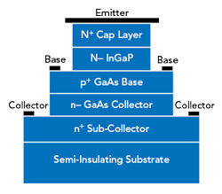
Figure 1 GaAs HBT cross-section.
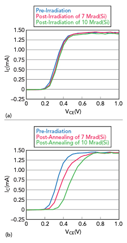
Figure 2 CE ICVCE characteristics pre-irradiation and post-irradiation (a) compared to pre-irradiation and post-annealing (b).