
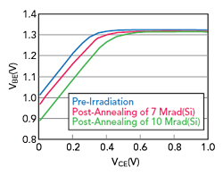
Figure 3 VBE vs. VCE for pre-irradiation and post-annealing.
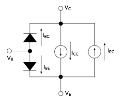
Figure 4 Modified Ebers–Moll model of a bipolar transistor.
The DC common-emitter ICVCE characteristics at 10 μA base current for gamma total doses of 7 and 10 Mrad(Si) are shown in Figure 2. Figure 2(a) compares the pre-irradiation and post-irradiation results, showing little variation of the collector current. Figure 2(b) compares the pre-irradiation, post-irradiation and post-annealing characteristics, showing notable changes in the collector current. One major effect of post-annealing is evident from Figure 2(b): VCE(sat) increases with increasing gamma total dose. VBE versus VCE at a fixed base current of 10 μA was measured before irradiation, post-irradiation and post-annealing (see Figure 3).
ANALYSIS
Why does VCE(sat) increase after annealing but not post-irradiation? Gamma irradiation possibly induces slow interface states at the interface between the air and insulating passivation layer that exchange charges with the semiconductor over a long time, which causes VCE(sat) to degrade as annealing time increases. The increase in VCE(sat) post-annealing may be understood by considering a modified Ebers–Moll model of the transistor (see Figure 4). IBE and ICC are the base and collector currents, respectively, caused by the forward injection across the base-emitter junction. These two components can be measured independently using forward Gummel measurements with VBC = 0. Similarly, IBC and IEC are the base and emitter currents, respectively, that are reverse injected by the base-collector junction. These can also be measured using inverse Gummel measurements with VBE = 0.
In the saturation region, where both the base-emitter and the base-collector are forward biased, the total collector current is given by

The inverse Gummel measurements show that IEC ≪ IBC, so IC is approximately

where VBEi and VBCi are the base-emitter and base-collector junction voltages, respectively, ICCS and ηBE are the saturation current and ideality factor of the collector current from the forward Gummel measurements. Similarly, IBCS and ηBC are the saturation current and ideality factor of the base current from the reverse Gummel measurements. The junction voltages may be different than the terminal voltages because of the voltage drops across the parasitic series resistances RE, RB and RC of the emitter, base and collector, respectively.

The collector-emitter saturation voltage, VCE(sat), is given by

where VBE and VBC are obtained by solving Equations 3 and 4, respectively. This gives

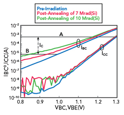
Figure 5 Inverse Gummel IBC and forward Gummel ICC characteristics pre-irradiation and post-annealing
These equations provide physical insight for understanding the gamma irradiation-induced increase of VCE(sat). The measured values of ICC versus VBE and IBC versus VBC are plotted in Figure 5. Two horizontal lines, A and B, are drawn at the values of VBE and VBC determined, respectively, from Figures 2(b) and 3 and Equation 5 at IC = 0.5 mA. In this case, the HBT operates in the saturation region, so VCE(sat) is simply the horizontal voltage separation between VBE and VBC.
Figure 5 shows that ICC increases slightly after annealing, the increase with gamma dose due to the increased saturation current of the base-emitter junction. This is caused by the large number of radiation-induced defects, causing amphoteric interface states to serve as efficient generation/recombination centers. On the other hand, the base current, IBC, in the inverse Gummel plots increases significantly after annealing, the increase in gamma dose is due to additional recombination in the SCR and quasi-neutral region. The increase of VCE(sat) is caused by the increase in current injected by the base-collector junction; the physical mechanism is discussed by Shatalov et al.8
The physical mechanism responsible for the increase of base-collector junction saturation current can be further understood by analyzing the base current, IBC, in the inverse Gummel measurements. For SHBTs, IBC has two main components: 1) recombination of electron-hole pairs in the bulk of the SCR and along its periphery and 2) recombination of injected holes in the bulk of the neutral collector region and at the surface. In the Vertical Bipolar Inter-Company (VBIC) model, IBC is given by

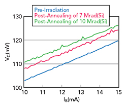
Figure 6 Fly-back measurement of VC vs. IB, showing emitter resistance, RE.
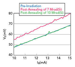
Figure 7 Fly-back measurement of VE vs. IB, showing extrinsic collector resistance, RCX.
IBC is the sum of two components: IBCi, modeled with a saturation current, IBCI, and ideality factor NCI ≈ 1 that comprises the neutral collector region recombination; and a non-ideal component for the SCR, modeled with saturation current IBCN and ideality factor NCN ≈ 2 for InGaP/GaAs SHBTs.
Using the data from the gamma total dose of 10 Mrad(Si) and the VBIC model in Advanced Design System, the non-ideal base-collector saturation current, IBCN, increases significantly from 5.06 x 10⁻¹⁴ A to 6.04 x 10⁻¹¹ A, and the ideal base-collector saturation current, IBCI, increases relatively slightly from 1.49 x 10⁻²⁰ A to 2.24 x 10⁻¹⁹ A. The observed increase in the saturation current of the base-collector junction appears to be mainly due to an increase of recombination current in the SCR.
Considering the effects of RC and RE in Equation 6 on the collector current after annealing, the first term, IERE, is proportional to RE, assuming IE is a fixed constant in this analysis. The total emitter series resistance is measured with the fly-back technique, where the emitter is grounded, current is forced into the base and the open circuit collector voltage is measured. The emitter resistance is the slope of the linear segment of the curve. Figure 6 compares RE from fly-back measurements for the GaAs HBTs before irradiation and after annealing. The figure shows almost no change in slope after annealing with 10 Mrad(Si) gamma irradiation, which means RE has not contributed to an increase in VCE(sat). The second term of Equation 6 represents the contribution from RC, the total collector series resistance, which includes the extrinsic collector resistance, RCX, and the intrinsic collector resistance, RCI, in the VBIC model. Figure 7 shows the RCX obtained from fly-back measurements, similar to the RE measurements shown in Figure 6. The value of RCX equals the slope of the linear segment of the curve, which changes slightly after annealing. RCI can be determined by optimizing the fit to the data from the common-emitter ICVCE characteristics of the quasi-saturation region. RC increases from 3.94 to 4.94 Ω with the irradiation dose of 10 Mrad(Si) due to an irradiation-induced carrier decrease in the neutral collector region. In the post-annealing following 10 Mrad(Si) gamma irradiation, the second term increases by only 8 mV, even with IC = 8 mA, which is the maximum IC of the test samples. Thus, the contribution of the parasitic series resistances to the increase of VCE(sat) is negligible, even at the maximum IC.
CONCLUSION
The collector-emitter voltage drop, VCE(sat), across the InGaP/GaAs SHBTs at saturation increases by more than 0.1 V after annealing gamma irradiation with a total dose of 10 Mrad(Si). From the analysis, the VCE(sat) increase is caused by irradiation-induced defects in the SCR and the neutral collector region. Experiments and analysis show that the defects in the SCR play a more important role increasing VCE(sat) than defects in the neutral collector region. With an increase in maximum IC, however, defects in the neutral collector region restrain the increase in VCE(sat) in gamma radiation environments.
Acknowledgments
This project was supported by the National Natural Science Foundation of China (Grant No: 61804046, 61704049), the Doctoral Scientific Research Foundation of Henan University of Science and Technology (Grant No. 400613480011) and the Foundation of Department of Science and Technology of Henan Province (Grant No. 202102210322, 192102210087).
References
- J. C. Zhang, B. Liu, L. M. Zhang, S. Ligong, W. Jinchan and L. Song, “A Rigorous Peeling Algorithm for Direct Parameter Extraction Procedure of HBT Small-Signal Equivalent Circuit,” Analog Integrated Circuits and Signal Processing, Vol. 85, No. 3, June 2015, pp. 405–411.
- J. C. Zhang, Y. M. Zhang, H. Lu, Y, Zhang, B. Liu, L. Zhang, J. Wang and L. Zhang, “A Ku-Band Low-Phase-Noise Cross-Coupled VCO in GaAs HBT Technology,” Journal of Circuits, Systems and Computers, Vol. 25, No. 6, January 2016.
- J. C. Zhang, Y. M. Zhang, H. L. Lu, Y. Zhang, B. Liu, L. Zhang and F. xiang, “A Ku-Band Wide-Tuning-Range High-Output-Power VCO in InGaP/GaAs HBT Technology, Journal of Semiconductors, Vol. 36, No. 6, June 2015.
- J. C. Zhang, B. Liu B, L. M. Zhang, J. Wang, Q. Hua, Y. Zhang, H. Lu and Y. Zhang, “A Ka-Band Low Phase Noise VCO Implemented in 1 μm GaAs HBT Technology,” Microwave Journal, Vol. 61, No. 11, November 2018, pp. 82–94.
- J. C. Zhang, M. Liu, J. C. Wang, L. Zhang and B. Liu, “Modeling of InP HBTs with an Improved Keysight HBT Model,” Microwave Journal, Vol. 62, No. 7, July 2019, pp. 56–62.
- J. Zhu, Z. Yang, W. Sun, Y. Du, Y. Sun, Y. Zhu, P. Ye and Z. Li, “Investigation on the Breakdown Failure in Stripe Trench-Gate Field-Stop Insulated Bipolar Transistor With Low-Saturation Voltage,” IEEE Transactions on Device and Materials Reliability, Vol. 16, No. 3, September 2016, pp. 384–387.
- A. Bandyopadhyay, S. Subramanian, S. Chandrasekhar and S.M. Goodnick, “Degradation of InGaAs/InP Heterojunction Bipolar Transistors Under High Energy Electron Irradiation,” IEEE International Reliability Physics Symposium Proceedings, March-April 1998.
- A. Shatalov, S. Subramanian and A. Klein, “Correlation Between Nonionizing Energy Loss and the Offset Voltage Shift in InP/InGaAs Heterojunction Bipolar Transistors,” IEEE Transactions on Nuclear Science, Vol. 48, No. 6, December 2001, pp. 2262–2269.