
There are several simultaneous trends enabling the transition of legacy applications, and creation of new applications, at mmWave frequencies. One of the most discussed reasons for this transition tends to be the overall congestion of sub 1 GHz and sub-6 GHz spectrum driving consumer and enterprise wireless communications toward higher frequencies. Though these lower frequency bands are certainly becoming increasingly used, the wireless standards operating at these frequencies are also becoming more capable of managing interference and standards are also driving stricter electromagnetic compliance (EMC) requirements to combat interference as a result of this congestion. Also, “intelligent” radio systems are also being developed with knowledge of the nearby EM environment, that can “choose” the best spectrum in which to operate given a specific payload of data or communication style.
Another possible reason is the increasing accessibility of precision manufacturing, lower cost and more compact computing resources, and simulation/model capabilities that can now tackle the small dimensions and dense physical structures of mmWave components and devices. Moreover, there are now RF semiconductor processes and circuit substrates (PCB, ceramics, and films) that can now more affordably offer higher power and performance at tens to hundreds of gigahertz.
The defense, aerospace, and satellite communications (Satcom) industries have relied on mmWave communications and sensing for decades to great effect. However, these industries tend to purchase components and devices in small volumes with extremely stringent sourcing, manufacturing, quality, testing, and documentation requirements. With more accessible mmWave design resources and RF hardware that can operate to these frequencies, developing and deploying mmWave communication and sensing technology is now seeing a much lower barrier to entry than in previous years.
How Do mmWave Frequencies Differ From RF or Microwaves?
The barriers to entry of developing and deploying mmWave communication and sensing technologies has largely been a result of the design and manufacturing complexity which tends to increase as a function of frequency. There are several key factors. mmWave devices and components are often necessarily proportionally smaller than lower frequency components and devices. An example of this is with ground planes for planar transmission lines, such as coplanar waveguides or striplines. It is generally recommended to use metalized via holes spaced at least 1/10 the wavelength apart to connect the multiple layers of grounds for good electrical connection and to prevent the development of undesirable transmission modes.
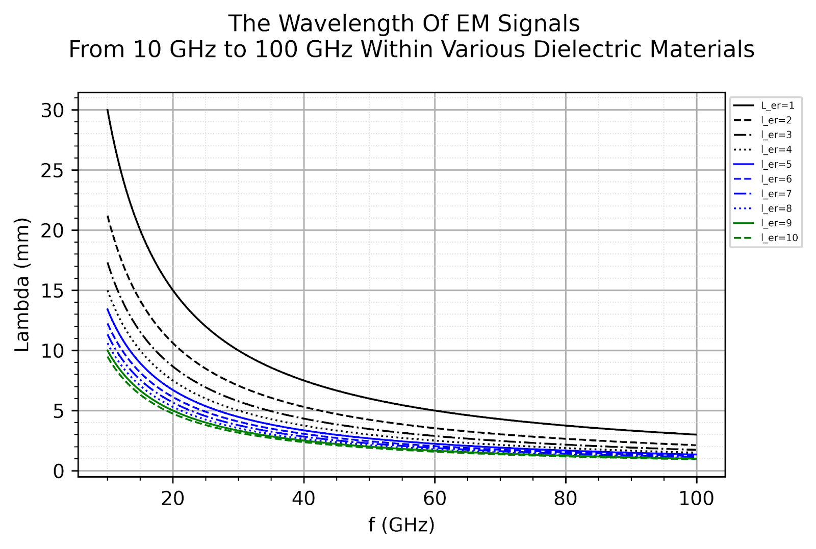
It can be observed from Figure 1, that 1/10 a wavelength of mmWave signals to 100 GHz in a dielectric media, such as a PCB substrate (~2 to 10 relative permittivity), are a fraction of a millimeter. Though this is certainly mechanically possible with some modern PCB, Low Temperature Co-fired Ceramic (LTCC), High Temperature Co-fired Ceramic (HTCC), thin-film, and thick-film fabrication processes, it has historically been at a premium cost. With ever denser digital electronics with digital signal data rates in the hundreds of gigabits per second (Gbps), PCB technology has subsequently enhanced to make manufacturing small precision traces, planes, and via holes more cost accessible and otherwise reliable.
Another factor to consider is that RF losses also tend to scale with frequency, or inversely to wavelength. Phenomena including skin effect, conductor losses, and dielectric losses are also a function of frequency. In the case of dielectrics, mmWave signals also react with dielectric boundaries with greater severity than lower frequency signals and are more readily absorbed by “lossy” dielectrics. The result of this is that mmWave signals face greater losses and scattering from common dielectrics in the environment, as well as dielectrics in building structures (such as concrete and insulation). Another side of this is that certain dielectric structures can also be used in similar ways to optical lenses and waveguides in manufacturable dimensions for mmWave applications. For instance, dielectric lenses can be used to focus, concentrate, or culminate mmWave radiation in a similar way that optical lenses manipulate visible light.
Atmospheric attenuation also depends on the frequency, with some portions of the spectrum suffering many times the loss of other bands in the nearby spectrum due to atmospheric phenomenon. The bands with the highest atmospheric attenuation also tend to be the bands available for license-free use or are otherwise unoccupied by military, defense, or Satcom restrictions (see Figure 2).
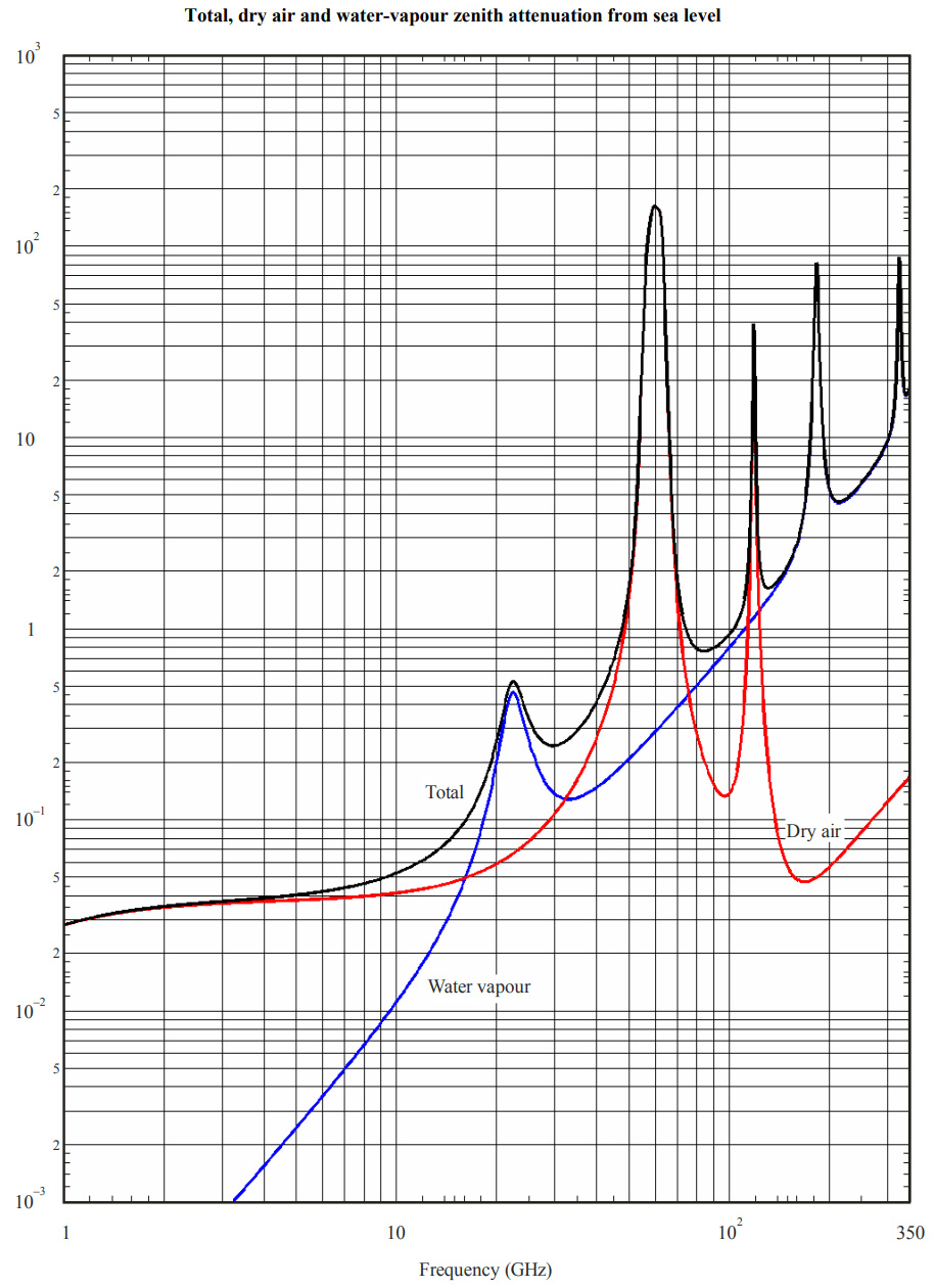
Figure 2. Total, dry air, and water-vapor zenith attenuation at sea level *Source ITU-R P.676-9 02/2012 (https://www.itu.int/dms_pubrec/itu-r/rec/p/R-REC-P.676-9-201202-S!!PDF-E.pdf).
Therefore, mmWave systems often require higher gain amplification and lower loss materials as part of their manufacture to overcome these losses. Fortunately, RF Front-end (RFFE) and antennas that operate in the mmWave have become increasingly integrated and more affordable, allowing for higher gain and lower loss mmWave components in smaller form factors and cost structures than in previous decades.
A caveat of this is that with higher gain, mmWave antennas are also necessarily more directive and therefore have a narrowing beampattern for transmission and reception. This is why AAS (Active Antenna Systems) are seen as an enabling technology for 5G, and future 6G, mmW technology. AAS using phased arrays or other beamsteering technology can provide higher gain and an antenna pattern that can be pointed at a target within a limited scanning angle of the antennas broadside face. The trade-off is that AAS requires more RF components in an often more compact space.
Fabrication Challenges
High RF Losses & Capacitive/Inductive Parasitics
The general guidance is that the effects of conductors, dielectrics, and semiconductor geometries on electrical performance are a function of frequency. Depending on the dimensions, there is a maximum frequency to which many of the EM effects (skin effect, dielectric loss, conductor loss, surface roughness, etc.) are negligible for a given structure and application. Due to the extremely small wavelength of mmWave signals, these frequency dependent effects generally must be considered.
For instance, the insertion loss impact of the skin effect, conductive losses, dielectric losses, and other possible effects like dispersion, increase with frequency. A transmission line of the same length tends to exhibit greater loss for higher frequency signals than lower frequency signals (see Figure 3).
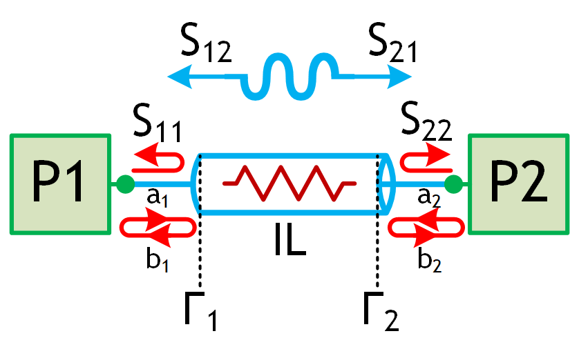
Figure 3. A 2-Port Network Diagram showing transmission (S12/S21), reflection (S11/S22), and Scattering parameter assignments with insertion loss of a transmission line depicted as an inline resistance.
Moreover, for many transmission line types, there is a maximum frequency for which the transverse-electromagnetic (TEM) or quasi-TEM mode are dominant, and higher frequency signals will experience additional transmission modes that could further reduce the performance of the transmission line.
The phase and velocity of propagation (phase velocity) of the signals passing through a transmission line are also a function of a variety of frequency dependent effects, including the surface roughness of the conductors used in fabricating the transmission line [2.1.2,2.1.3,2.1.4]. A result of this is that it is often a challenge to maintain the group delay (phase delay across a frequency band) for wide bandwidth signals, which is increasingly crucial for highly complex, modern modulation schemes.
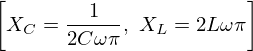
Where Xc (capacitive reactance), XL (inductive reactance), C (capacitance), L (inductance), ⍵ (frequency).
The capacitive (Xc) and inductive (Xl) reactance are also a function of frequency. This means that the effect of capacitive and inductive parasitics are more significant at mmWave frequencies, even though the inductance and capacitance values derived from electrostatic effects remain the same. This has a direct impact on the performance of mmWave field-effect transistors (FET), which suffer from frequency operation limitations due to the gain-to-drain parasitic capacitance being amplified by the Miller effect in some designs. This is also a challenge as reaching higher frequency operation also necessitates a shrinking of geometries, for which parasitic capacitances often increase as conductors and semiconductors become more closely spaced. In order to keep parasitic capacitances small at mmWave frequencies, dielectrics with low dielectric constants are used, such as in circuit substrates and coatings.
mmWave Minimum Physical Constraints
The size, tolerances, and repeatability of electrically significant structures at mmWave frequencies are key considerations when designing and fabricating mmWave components in devices. Certain fabrication processes that can only achieve trace and feature resolution to a few millimeters will likely be unsuitable for mmWave applications, which generally require trace width and feature sizes in the hundreds of micrometers (microns). With base feature sizes so small, the tolerances of the features also become more important. RF and microwave frequency fabrication processes may have manufacturing tolerances as high as the feature sizes for mmWave components and devices.
The EM field lines are also concentrated closer to the conductors and dielectrics of the physical structures, which further exacerbates the impact of manufacturing tolerances, surface roughness of conductors, and material property conformality at mmWave frequencies. Using planar transmission lines and waveguides as examples, the efficient transmission of signals through these signal carrying lines depends on the exact dimensions ratios of the geometries.
If a 60 GHz stripline with a strip width in the hundreds of microns and substrate height also in the hundreds of microns, suffers from stripe width or substrate thickness tolerances in the tens of microns, then the characteristic impedance of the stripline can be thrown off by over 10% at any given cross section along the stripline. This would amount to creating additional reflections and the development of standing waves within the stripline that could dramatically reduce the transmission lines performance. Maintaining an acceptable impedance tolerance with such a stripline may require geometric tolerances on the micron level and material conformality to less than 1% deviation. This is generally beyond what can be done with PCB manufacturing, which typically has minimal trace widths and spacing around 76.2 micrometers (0.003”) with tolerances in the 10s of micrometers. Other non-semiconductor fabrication technologies for RF structures (LTCC, thin-film, thick-film, etc) also have tolerances limits from several micrometers and upward. This is why manufacturing circuits for high-speed digital and RF devices often requires special attention and sacrificing of absolute dimensional accuracy for relational accuracy between specific critical dimensions, such as the trace width and spacing to ground traces for coplanar waveguides.
Summarily, to fabricate mmWave devices and components, the manufacturing tolerances, surface roughness, and material property conformality requirements must become proportionally tighter as frequencies increase. This also directly applies to repeatability where the tolerances stackups and material property deviations could also lead to components and devices within a batch to vary considerably.
mmWave Material Constraints
The level of manufacturing sophistication needed to reliably produce some mmWave components and devices is available in semiconductor manufacturing, where dimensions and features can be on the sub-nanometer scale and high volume production is possible with an emphasis on repeatability. However, the processes of designing a semiconductor component/device or otherwise producing a mmWave part generally requires access to design and production experts familiar with such part manufacture and access to specialized manufacturing equipment/processes. In some cases the equipment or technology needed for mmWave component or device development may even be under export control and access may be limited to the necessary technology in some regions of the world.
Furthermore, there are fewer material choices for conductors and dielectrics that can be fabricated to the necessary sizes, tolerances, and conformality requirements for mmWave. There is also often a vertical market of services that are needed to produce mmWave technology. For instance, producing ceramics that can be used for LTCC, HTCC, thin-film or thick-film mmWave circuits often requires first sourcing the ceramic substrate, lapping/polishing, machining the substrate to appropriate size sections for the application, adding metallization, plating the metallization, and other steps for which there may only be one or a few available regional suppliers/vendors. Consequently, developing a mmWave technology often involves overcoming design and production challenges at each stage of the vertical, that further increase overall system costs and lead to longer design and production cycles (i.e. time-to-market). This is a major area of innovation and academic research with teams and organizations round the world developing new solutions and demonstrating prototypes, such as nScrypt, Nano-Fabrica, Nuvotronics, and many others. Though capable, these new technologies and approaches tend to fall short in the task of developing relatively large volume dielectrics at high resolutions with extreme levels of material property control.