
Dielectric Specific Fabrication Challenges
Where conductors are formed of metals, which can generally be reliably deposited, sputtered, formed, and plated to reasonably high tolerances and readily measured, dielectrics are most often ceramics, glasses, or polymers, which often present their own nuanced production and manufacturing challenges. The most significant electrical characteristics of conductors at mmWave is generally the surface of a conductor, depending on how thick the conductor is and the relative depth of the carrier concentration, which can be plated or otherwise coated with gold or other noble metals to provide for higher conductivity and more conformal outer surface.
For dielectrics, which are often used to support, separate, or load conductive structures, the surface and bulk of the dielectric are critical and the electric field typically penetrates into, or through, the entire dielectric. As the electric field passes through a dielectric, some of the overall energy is absorbed (dielectric loss tangent, or its reciprocal, quality factor) and converted to heat. For many dielectrics, a relatively small change in temperature can result in a change of the overall dielectric performance and dimensional stability of the dielectric structure. Consequently, dielectrics with extremely low loss tangents, less than 10^-4 at 1 kHz and 10^-3 in the mmWave are desirable [2.1.5].
Conformality of the dielectric properties and dimensions of dielectrics are subsequently critical, as even small variations or gradients of the dielectric performance of the material can change the behavior of the electric field passing through the dielectric. Spatially layering or mixing dielectric materials result in generally difficult to determine dielectric effects which may result in the effective permittivities of a given dielectric structure to be much different than the dielectric performance of the individual dielectrics. For instance, in a parallel plate capacitor, the direction of the dielectric layers in respect to the capacitive plates determines the effective permittivity of the overall dielectric. For perpendicularly stacked dielectric layers the effective dielectric is essentially cumulative, where parallel stacked dielectric layers (perpendicular to the electric field with equal charge) results in an effective permittivity which is the cumulative of the reciprocals of the layer’s dielectric constant (see Figure 4). For more complex 3d structures, this computation becomes increasingly complicated, and thus hard to analytically determine (i.e. using effective medium theory).
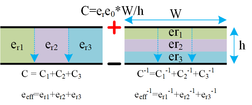
Figure 4. Parallel plate capacitor with series and parallel dielectrics.
Thus dielectrics for mmWave technology need to be machined, deposited, developed, or layered with exacting precision, and such precision effectively acts as a limiting factor to what materials and fabrication processes may be viable for a given mmWave frequency. An important note is that this behavior of dielectrics can be intentionally exploited to develop dielectric metamaterials and metasurfaces. A new class of electromagnetic metastructures (metamaterials, metasurfaces, meta-atoms, metalfilms, metascreens, etc) can be made to behave in ways that traditional dielectrics in nature, or as conformal bulk structures, cannot.
Essentially, within a dielectric medium, the dipole moments are induced by the electric polarizabilities of the scatterers embedded within a medium when exposed to an electric field [2.1.6]. By volume averaging the dipole moments into a polarization density (P) and the electric field (E), the result is an electric displacement vector (D) and permittivity (epsilon):

Though natural dielectrics and materials only have positive values for permittivity, man made materials with special properties or structures have since been made/arranged in such a way as to yield a negative refractive index, or negative permittivity. This is also the case for other classes of magnetic metastructures impacting the magnetic permeability, but that is beyond the discussion of this paper. An interesting note about these metastructures is that the nontraditional permittivity behavior is frequency dependent, where frequencies outside of the range of the structures interact with the structure in more traditional ways. In this way these materials behave as a continuous effective medium with bulk effective material properties. Within that frequency range of operation, composite/engineered materials can result in effects that dramatically change the electric performance of the structure.
For instance, creating a grade of refractive indices within a dielectric volume can result in behavior that physically resembles that of optical lenses, but on electromagnetic radiation well below that of visible light. These gradient refractive index (GRIN) structures can be specifically designed to act as complex optical structures that yield a desired radiation pattern from that of traditional lenses, and also more complex and nuanced behavior.
Other mmW metastructures can be fabricated that allow for amplitude and phase manipulation, near-field interactions, and even nonlinear behavior depending on the design and materials involved. A main advantage of mmWave metastructures is the enhanced degrees of freedom and more compact dimensions that can result from periodic, unit cell, or fractal metastructure design methods.
The precision and tolerance of the manufacturing process are intrinsically significant with 2D and 3D mmWave metastructures, as the structures require structure sizes on the order of fractions of a wavelength and tolerances a few percent of that minimum structure size. Otherwise, such a mmWave metastructure would operate less efficiently, or even fail to function as intended.
This is a particular challenge with dielectrics, as there are limited manufacturing processes that can produce ceramic and glass structures with such small dimensions, conformally, and with tight tolerances [2.1.5-2.1.10]. Furthermore, to achieve other performance goals, these metastructures also need to be constructed of materials with extremely low dielectric losses (loss tangent), which rules out many polymers and other materials. Composite materials can be produced with the desired behavior and assembled through additive manufacturing approaches. However, there are few additive manufacturing processes that are compatible with complex dielectric composite materials that can produce relatively large dielectric structures (centimeters) with high resolution features (tens of microns). There are promising new composite materials and fabrication approaches that use innovative methods to ensure conformal mixing, hence material properties, and can produce structures on such scales as to be useful well into the mmWave frequencies such as what Fortify is doing with Rogers materials.
Integration Challenges
With increased accessibility to mmWave technology has come the desire to embed and integrate mmWave devices and systems in a variety of form factors and in applications that don’t have the power or space available for traditional mmWave systems composed of discrete mmWave components. As a result, there is increasing incentives for manufacturers to enhance the level of integration of mmWave components, devices, and systems. To overcome the high atmospheric attenuation and other intrinsic RF losses within a mmWave system, much of the effort in realizing viable mmWave systems has largely been on integrating and developing enhancements to AAS.
mmWave Integration Design Considerations
- EMC/EMI close proximity & high component densities
- Complex signal routing requiring high performance transmission line or waveguide interconnect
- Analog, digital, power, and RF coexistence
- Thermal management
- Power Routing
- Enclosure/housing that doesn’t lead to unintended effects
- Integrating microwave and mmWave antennas/structures without sacrificing gain
- mmWave AAS Specific Challenges
For instance, previous generations of mmWave communication (mainly backhaul, radar, and Satcom), were generally built with digital signal processing and networking electronics that were highly integrated, and mmWave electronics that were assemblies of discrete mmWave components and devices. Such assemblies are often composed of discrete power amplifier pallets, a monolithic microwave integrated circuit (MMIC) low noise amplifiers, mixers, local oscillators (LOs), switches, circulators/isolators, power divider/combiners, and transmission line/waveguide based interconnect. Depending on the application, the filters in the system may be discrete, connectorized, or contained within their own integrated microwave assembly (IMA) as a filter bank. In some cases, these integrated modules have performance requirements that necessitate specialized interconnect, such as wire bonding or using coaxial spring probe connector assemblies between integrated modules.
With the advent of 5G beamsteering and multi-input multi-output (MIMO) systems, actively electronically steered antenna arrays (AESAs), and phased array-based Satcom systems, the number of RF Front-ends (RFFEs) and interconnects have been increased. Hence, a new level of mmWave integration is needed. In many cases, design teams have turned toward semiconductor, thin-film/thick-film, LTCC, and other highly compact integration processes to even further compress the overall size of mmW components and devices in a system.
mmWave Integration Technologies
- MMIC built with silicon or III-V type semiconductors
- LTCC or mmWave PCB with System-in-Package (SiP) RFFE hardware
- Integrated Microwave Assemblies (IMAs) that use suspended substrate (SS), LTCC, thin-film/thick-film, or other compact components/devices
- Heterogeneous or 2.5D/3Dintegration of class III-V semiconductor devices and silicon (Si) complementary metal-oxide semiconductor (CMOS) devices, similar to silicon-germanium (SiGe) BiCMOS processes, for the development of digital/RF systems-on-chip (SoCs).
- Micro-electromechanical systems (MEMS) switches, filters, phase shifters, attenuators, etc.
- Digitization of modulation, demodulation, frequency conversion, filtering, and signal enhancing features
The move toward beamsteering antenna and other AAS technologies has also resulted in the addition of mmWave signal chain components that require integration, mainly variable attenuators/amplifiers and phase shifters. Though more capable digital signal processing (DSP), FPGAs, application specific integrated circuit (ASIC), central processing units (CPUs), analog-to-digital converters (ADCs), and digital-to-analog converters (DACs) are now capable of sophisticated signal synthesis, manipulation, and conversion, these digital electronics are not able to fully address the RF performance requirements from the RFFE onwards in the signal chain. This is why there is still substantial investment in developing more compact and capable mmWave components and devices and to enhance the interoperability of these technologies for wider applicability [2.2.4-2.2.7]. For many mmWave applications, direct-digital-conversion (DDC) and direct-digital-synthesis (DDS) electronics are not capable of synthesizing or converting to the desired mmWave operating frequencies, and there is often still a need for frequency conversion devices beyond 6 GHz (X-band and beyond). Consequently, the RFFE and antenna systems for AAS still consume a significant amount of the power, space, cost, and design complexity budget of a mmWave system and are often a limiting factor in the performance and capability of modern system (see Figure 5).
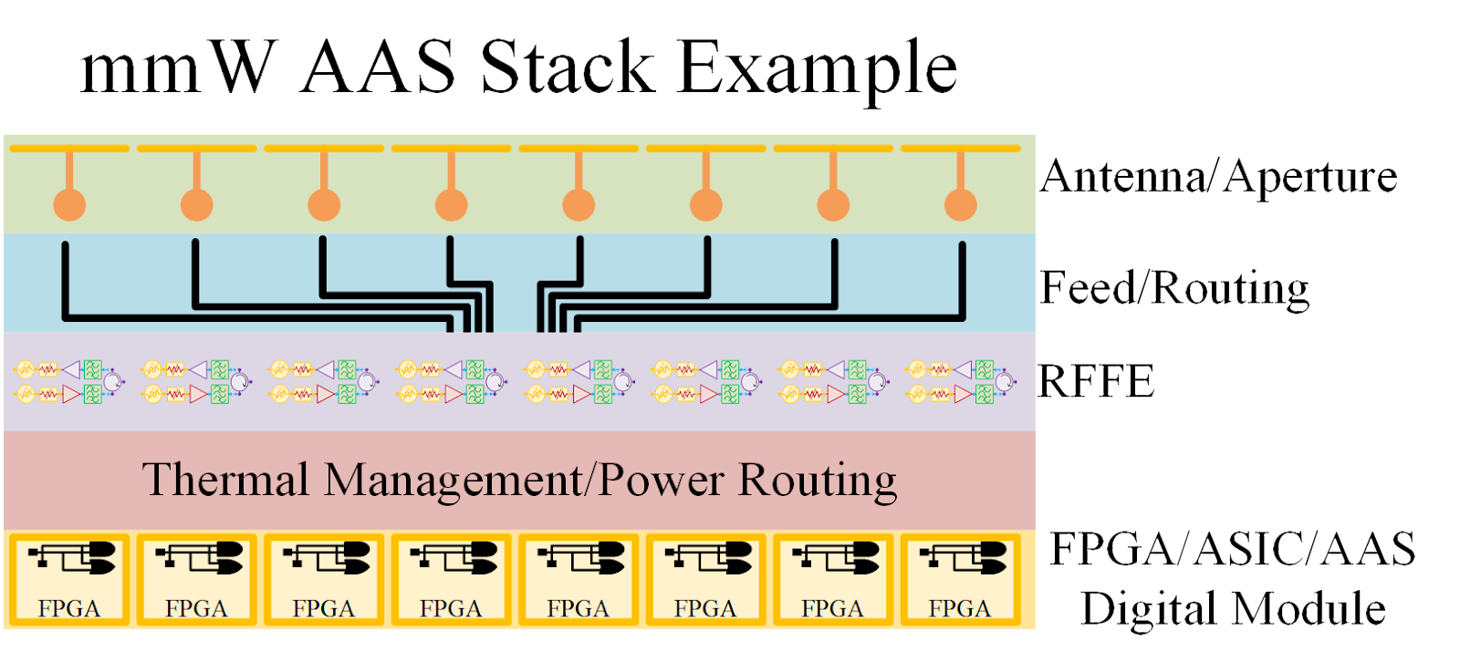
Figure 5. An example of a highly integrated antenna array stack built as a layered module.
To achieve the desired operating range, throughput, or resolution in a given size and power budget with an AAS, there is substantial emphasis on power amplifier efficiency and receiver dynamic range [2.2.4-2.2.7]. For example, the F-22 Intra-Flight Data Link (IFDL) upgrade, the F-35 Multi-function Advanced Data Link (MADL) is designed using an active analog beamformer with the assumption that the extremely narrow antenna beams and high atmospheric attenuation of mmWave system provides enhanced physical security and shorter multi-beam neighbor discover times.
In much the same way, 5G AAS are relying on thin mmWave links to establish extremely high data rates, and face many of the same challenges of getting the most from highly integrated RFFE signal chain components. Therefore, methods of improving the antenna gain, efficiency, or directivity of the AAS without sacrificing, and even enhancing, the maximum scanning angle can lead to improved overall mmWave AAS performance or alleviate some of the performance requirements from the RFFE hardware. Accordingly, dielectric metastructures that can reduce side-lobe levels, enhance the maximum scanning angle, and/or improve antenna efficiency may provide benefit in the design of mmWave AAS to meet these latest challenges, be it for aerospace/defense, Satcom, or telecommunications [2.1.11].
Complex Dielectric Specific Integration Challenges
In order to benefit from dielectric metastructures, they must be carefully designed as a key feature of an AAS, or as an enhancement addon. Either way, the design and fabrication of the dielectric metastructure, in the majority of cases, will need to be customized to a given design. This is because virtually every physical dimension of a dielectric metastructure needs to be designed in respect to the desired function of the structure. Unlike a radome, which is mainly a necessary protection of a radar/communication external hardware but doesn’t necessarily benefit the function of the system, dielectric metastructures in such systems are key components that critically change the behavior of the electric fields within a mmWave system or radiated/received by the system [2.2.8,2.2.9].
Integration of dielectric metastructures, in most cases, will require full EM simulation and optimization of the mmWave system as it will be integrated to fully determine the end-design. This is due to the impact of the design integration and fabrication of the integrated assembly on the radiation and the electric field behavior within a device and from it's antenna structure. This type of simulation is computationally expensive for mmWave structures of any size or complexity, as the mesh refinement and resolution required to achieve accurate simulation results is quite sophisticated. Optimization of a dielectric metastructure could require a substantial amount of time, as iterative simulation refinement may be needed. It is also likely necessary in order to characterize the behavior of the lens feed system, for a dielectric lens antenna, or the placement and fixture tolerance within the assembly housing [2.2.10,2.2.11].
Manufacturing dielectric metastructures for integration with a mmWave system applications using traditional layered, cast/molded, or CNC subtractive manufacturing approaches may also incur significant expense and development of tooling, dies, molds, etc. Consequently, there is an active tradeoff between the time and resources spent on design optimization and manufacturing optimization, either of which have their own expense considerations, risk, and unknowns. Therefore, it is likely desirable to have access to flexible methods of fabricating dielectric metastructures with a high degree of design flexibility and tight manufacturing tolerances. These are both achievable with recently developed dielectric materials and digital light processing (DLP) 3D printing technology [2.1.11].
Conclusion
There are a slew of market forces and technology trends that are driving development of wireless communication and sensing systems designed to operate in frequency bands previously only used in satellite communication, backhaul, and military radar. An example of this is the recently released and licensed 5G and Wi-Fi frequency bands beyond 6 GHz, as well as the extended V-band allowing unlicensed use to 71 GHz. With the growing spectrum congestion below 6 GHz, many applications are being redesigned to operate at higher spectrum regimes, which in turn, is causing yet other applications to seek even further heights of spectrum to avoid interference.
There are also other attractive features of operation at mmWave frequencies, namely that the size of many RF electronics scales in proportion to wavelength. mmWave components and devices can often be fabricated in much smaller form factors than lower frequency components and devices (i.e. smaller antenna and other RF hardware). Examples of this include mmWave 5G gnodeB and antenna array, as well as mmW sensing devices, such as mmW imaging systems and radar.
This is a double-edged sword of sorts, as the relative sizes of mmWave hardware shrinks, the manufacturing tolerances and precision material requirements become stricter proportionally due to a variety of phenomenon (skin effect, high RF losses). Though the promise of broad swaths of available spectrum in the mmWave frequencies seems attractive, there are many phenomenon and fabrication considerations that come into play at these frequencies that are often either negligible or ignored at lower frequencies. There are also some technologies, now emerging, whose benefits could not fully be realized below mmWave frequencies, such as dense active/advanced antenna arrays (AAS). Now is the dawn of mmWave emerging from the shadows into mainstream use, as well as the emergence of mmWave design and fabrication challenges that may require designers to step outside of their familiar solutions to solve.
References
- Introduction
- The Trend Toward Millimeter-waves
- How Do Millimeter-wave Frequencies Differ From RF or Microwaves?
- Fabrication, Design, & Integration Challenges For Millimeter-wave Devices
- Fabrication Challenges
- Semiconductor technologies for 5G implementation at millimeter wave frequencies – Design challenges and current state of work
- PCB Design and Fabrication Concerns for MILLIMETER-WAVE CIRCUITS
- Effect of conductor profile on the impedance and capacitance of transmission lines
- Transmission Line Loss Properties of Dielectric Loss Tangent and Conductive Surface Roughness in 5G Millimeter Wave Band
- Silicate dielectric ceramics for millimetre wave applications,
- Dielectric Materials for Wireless Communication
- Dielectric Metamaterials
- Dielectric Metamaterials and Metasurfaces in Transformation Optics and Photonics 1st Edition
- Integrating microsystems with metamaterials towards metadevices
- All-Dielectric Metamaterial Fabrication Techniques
- 3D Printed Dielectric Lenses Increase Antenna Gain and Widen Beam Scanning Angle
- Integration Challenges
- Packaging Trends for Millimeter-Wave Radar and Communication Systems
- Stacking GaN And Silicon Transistors On 300 Mm Silicon
- Packaging and Antenna Integration for Silicon-Based Millimeter-Wave Phased Arrays: 5G and Beyond
- The Microwave and Millimeter Wave Integrated Circuit (MIMIC) DARPA
- Millimeter Wave GaN Maturation (MGM) DARPA
- Millimeter Wave Digital Arrays (MIDAS) DARPA
- The DARPA Millimeter Wave Digital Arrays (MIDAS) Program
- Effect of dielectric materials on integrated lens antenna for millimeter wave applications
- Modeling and validation of a mm-wave shaped dielectric lens antenna
- Review of 20 Years of Research on Microwave and Millimeter-wave Lenses at “Instituto de Telecomunicações”
- Multi Beam Dielectric Lens Antenna for 5G Base Station
- Fabrication Challenges