
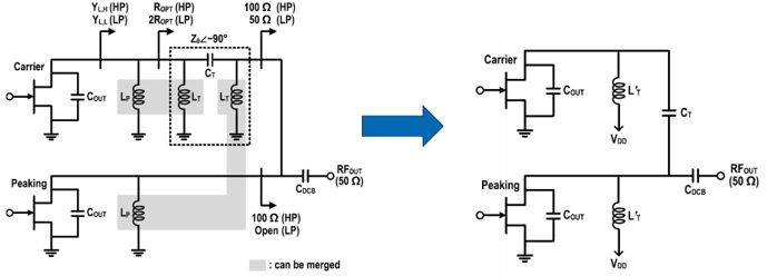
Another output matching circuit lumped CLC quarter-wave topology aims to remove the conventionally leveraged offset line in the peaking amplifier in order to meet the size constraints for mMIMO applications. Typically, DPAs will include a quarter-wavelength offset line in the carrier amplifier and half-wavelength offset line in the peaking amplifier after the output matching networks for proper load modulation and wideband performance. This replacement is accomplished by instead using a series inductor (Lp1), a shunt inductor (Lp2), and a series capacitor (Cp1) after the peaking amplifier (Figure 5). This way, both the frequency dependent compensation functions that the offset lines provide and the output matching functions can be combined into a more simplified, space-constrained circuit. In this circuit, the impedance at power backoff ![]() has a similar frequency characteristic to that of a half-wavelength line that acts as an open stub at the center frequency, is inductive at lower frequencies, and capacitive at high frequencies. Moreover, the impedance of the peaking amplifier at saturation
has a similar frequency characteristic to that of a half-wavelength line that acts as an open stub at the center frequency, is inductive at lower frequencies, and capacitive at high frequencies. Moreover, the impedance of the peaking amplifier at saturation ![]() can be transformed into any real impedance lower than the optimal impedance of the peaking amplifier
can be transformed into any real impedance lower than the optimal impedance of the peaking amplifier ![]()
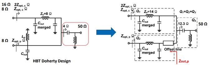
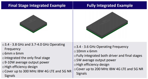
In implementing this topology, the bonding wires connecting the peaking FET and the circuit are included in the value of Lp1 while series bonding wires from the carrier FET is included in the output matching network with Lc1, Lc2 while the offset line is formed by the transmission line TLc1 (Figure 5b). This leads to a 10mm by 6mm package (after molding) that is implemented on a multilayer epoxy substrate. Final drain efficiencies stand at 53.7% and PAE at 44.8%, both at 8 dB backoff, while the peak output power is 45.3 dBm, and gain is 28 dB (at 8 dB backoff).
Lumped LCL Quarter-Wave Topology
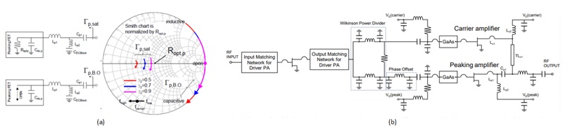
In some lumped LCL topologies, both the input and output include harmonic control circuitry to match the harmonics of the output impedance for the carrier and peaking amplifiers with the optimum impedances for drain efficiency [7].
Quasi-lumped Quarter-wave Topology
The quasi-lumped, quarter-wave architecture compensates for the output capacitance of the carrier and peaking amplifiers incorporating it in a transmission line, ultimately forming an impedance inverter. This way, by choosing the right length and characteristic impedance of the artificial transmission line the output capacitances and the bond-ware capacitance can be absorbed. And, rather than be limited by the bandwidth of the conventional half-wavelength transmission line impedance inverter and the bandwidth of the parallel resonator (inductor) that is typically used to eliminate the output capacitances [2]. However, this asymmetrical DPA design can lead to sensitivity issues due to the difference in output capacitances between the carrier and peaking amplifiers.
Wolfspeed GaN on SiC Integrated Power Amplifiers for mMIMO
There are some general conclusions that can be gleaned from the previous topologies aiming for an integrated DPA approach. They are as follows:
- The need for a relatively large load impedance
- The need to achieve an adequate load modulation of the carrier amplifier through a 90o phase circuit
- The need to achieve a high output impedance in the peaking amplifier to minimize the power leakage to the FET while ensuring a phase relationship with the carrier amplifier
With all of these considerations there is a general challenge of integrating the phase compensation network, input matching and output harmonic control circuit together on the input side of the DPA. On the output side, combining the output matching network for proper load modulation as well as replacing the offset lines and quarter-wave transformer with discrete inductors and capacitors for comparable wideband performance is the design challenge.
Wolfspeed integrated DPAs offer two topologies (Figure 8) [8]:
- A final stage integrated PA (includes only final stage)
- Fully integrated PA (includes both driver and final stages)
Conclusion
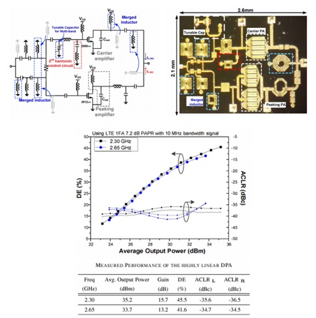
The various 5G infrastructure trends have led to tighter design tolerances with advanced radio techniques, higher performance requirements, tighter restrictions, and more integration. There is a general call for a higher degree of modularity, PAs for mMIMO are no exception to this trend, where PAs are expected to achieve both a high linearity and efficiency all within a small form factor. This leads to the need for an integrated DPA where a number of design challenges crop up when both minimizing and combining the input and output circuits of the carrier and peaking amplifiers while achieving broadband performance. The GaN HEMT using the GaN on SiC is a promising candidate for the integrated DPA with several advantages including a wide bandwidth performance and the ability to achieve higher efficiencies than other technologies. Wolfspeed 5G mMIMO GaN on SiC integrated PAs show high linearity and efficiency under wide bandwidth signals ― all within a small form factor.
- Seunghoon Jee, et al., “GaN MMIC Broadband Doherty Power Amplifier,” APMC 2013
- J. H. Qureshi, et al., “A Wide-Band 20W LMOS Doherty Power Amplifier,” IMS 2010
- Hwiseob Lee, et al., “Highly Efficient Fully Integrated GaN-HEMT Doherty Power Amplifier Based on Compact Load Network,” TMTT 2017
- S. Sakata, et al., “A Fully-Integrated GaN Doherty Power Amplifier Module with a Compact Frequency-Dependent Compensation Circuit for 5G massive MIMO Base Stations,” IMS 2020
- Daehyun Kang, et al., “Design of Bandwidth-Enhanced Doherty Power Amplifiers for Handset Applications,” TMTT 2011
- Seunghoon Jee, et al., “A Highly Linear Dual-band Doherty Power Amplifier for Femto-cell Base Stations,” IMS 2015
- Yunsik Park, et al., “GaN HEMT MMIC Doherty Power Amplifier With High Gain and High PAE,” MWCL 2015
- Jangheon Kim, et al., “GaN-on-SiC Integrated Power Amplifier for 5G Multi-User Massive MIMO Application,” EuMW 2020.