Abstract
The race towards hitting 5G speed, capacity, and availability requirements has come with it a number of nascent foundational technologies. At the forefront of these innovations is massive Multiple-Input Multiple-Output (mMIMO), or the outfitting of a base station with hundreds to thousands of antenna elements, each with its own respective transmit/receive signal chain, to maximize spectral efficiency.
The realization of mMIMO requires a high degree of integration with all components in the transceiver, including the power amplifier (PA). This article discusses the various 5G trends and challenges of mMIMO with a dive into the varying integration topologies for the commonly used Doherty Power Amplifier (DPA). Finally, an introduction to Wolfspeed fully integrated PAs is made by showing good RF performance over wide bandwidths.
5G Infrastructure Trends
Changes in xHaul
In the past, older iterations of 4G base stations (eNodeB) would involve antennas connected to remote radio heads (RRHs) at the top of a cell tower for PHY layer processing that was attached to the baseband unit (BBU) for more complex signal processing. On the network level, multiple RRHs could be served by a pool of BBUs at a far-edge location via the CPRI protocol over a fiber optic link. This centralized RAN topology (C-RAN) has shifted towards a disaggregated network architecture to better fit the varying traffic, throughput, and latency demands of a location. Instead, the 5G architecture involves a function split between the Centralized Unit (CU) and a series of Distributed Units (DU), with the additional potential split of a Radio Unit (RU). In this split, the DU handles low-latency, real-time traffic, while the CU handles non-real-time protocols. This allows for a higher throughput and lower latency communications with a lower layer split (Intra-PHY split). It is known that this split is required in order to support some advanced radio techniques such as Carrier Aggregation (CA) and Coordinated Multipoint (CoMP). For this reason, the enhanced CPRI (eCPRI) protocol was released to better support this functional decomposition.
PA Design Challenges with Advanced Radio Techniques
Power Amplifier (PA) design has been increasingly difficult with modern cellular systems ― the OFDM modulation scheme has a high peak-to-average power ratio (PAPR) of around 8-10 dB. This, in turn, requires the amplifier to stay at backoff, well within the linear region to meet adjacent channel power ratio (ACPR) or adjacent channel leakage ratio (ACLR) requirements. The issue with this is when the PA must function within its linear region and away from saturation (its non-linear region), it does not function nearly as efficiently. The use of CA involves the aggregation of available contiguous or non-contiguous blocks of spectrum to increase the throughput and latency of wireless communications in what is typically a populated spectrum (sub-6 GHz). This requires the amplifier to be at additional backoff to avoid the interference of two non-contiguous carriers transmitting simultaneously and to meet strict emissions requirements. Additionally, the amplifier must operate within a wide instantaneous bandwidth, creating a much more complex design challenge to meeting ACLR requirements while maintaining a nominal efficiency.
Linearization/efficiency enhancing techniques
These problems have led to the increased utilization of linearization and efficiency enhancing techniques. The Doherty amplifier configuration is amongst the most popular efficiency enhancing methodology for relatively high PAE deep into the output backoff region. Linearization enhancing methods includes digital predistortion (DPD) where the PA is able to operate near saturation without causing nonlinearities. This is accomplished by distorting the input in such way that the distortions at the output are minimized to increase linearity without compromising PAE.
mMIMO & The Need for Integration
Architectural Challenges of MIMO
MIMO has been leveraged for some time now in either a passive antenna topology or an active antenna system (AAS). The issue with passive antenna structures is the increase in channels (e.g., 4T4R, 8T8R, 16T16R, 32T32R), which is directly correlated to a larger antenna count and leads to an increasingly higher port density at the antenna. This, in turn, leads to an array of installation issues as well as unwanted signal degradation from the increasing presence of potential Passive Intermodulation distortion (PIM) sources (e.g., coaxial connector heads). The complexity of this problem only increases with mMIMO. This is where the AAS architecture provides a more optimal solution with an integrated antenna/radio, the only connections that are required to the system are a fiber and DC link for power and control. This differs from older base station architectures where a multi-port passive MIMO antenna structure would be connected to an RRH to finally be routed to the BBU.
mMIMO PA Design Challenges
mMIMO has with it, its own design challenges. Each transceiver chain must be optimized to minimize the inevitable losses, emissions, and non-linearities that will occur. The PAs in this system must then meet linearity requirements while also considering amplifier efficiency, all in a very integrated system package. The typical use of linearity and efficiency enhancing techniques to better meet ACLR requirements without compromising efficiency greatly involves added circuitry which is not typically integrated into the PA package. This is a significant consideration for mMIMO systems as any additional real estate used at the component-level compounds at the system-level with massive number of antennas and respective transmit/receive chains. An integrated PA design with the most commonly leveraged Doherty configuration and DPD linearization technique can be highly beneficial for system engineers in the installation of mMIMO. This can then afford the designer more flexibility in terms of the basic design requirements on power, size, weight, and cost.
Benefits of Using GaN
The use of GaN transistors has already permeated the wireless industry for large, macrocell high powered amplifiers (HPA) and is well positioned to overtake the popularized Si-based LDMOS PA that was previously leveraged. This is due to the intrinsic benefits this substrate has for power applications ― the wide bandgap, combined with its high breakdown electric field, power density allow for the handling of large powers all while exhibiting a sufficient electron mobility and saturation velocity to operate at high frequencies. Ultimately this increases the device's reliability, as the amplifier is able to withstand higher junction temperatures for longer periods of time. GaN transistors are capable of this all within a smaller package and at higher frequencies (DC-40 GHz) as manufacturing techniques advance with large wafer diameters and increasingly smaller gate-lengths (e.g., 0.25μm, 0.15μm) fabrication processes. GaN HEMT technology, in particular, has the capability of achieving a higher efficiency at high frequencies, over a wide bandwidth.
Discrete vs Integrated Doherty Power Amplifiers
As mMIMO calls for an increase in integration, smaller form factors are demanded with a high level of linearity and efficiency over a wide bandwidth. Integrating the popularized Doherty PA configuration to enhance efficiency would minimize the 5G New Radio (NR) size and weight and ultimately yield large space savings on the macro-scale in mMIMO installations (See Figure 1). The benefits of small form factor and ease-off-integration come with a number of design considerations though ― chief among them, the operating frequency and operating bandwidth of integrated PAs are fixed. Still, this design constraint can be relaxed by minimizing the bandwidth limitation of the quarter-wave transformer, phase compensation, and the offset lines found in the Doherty configuration.
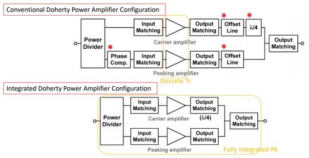
Figure 1: Discrete (top) versus integrated (bottom) transistor configurations. Maximal bandwidth can be achieved in the integrated example by minimizing the bandwidth limitations of the quarter-wave transformer, phase compensation, and offset lines. Image Link
The discrete transistor topology (Figure 1a) has the inherent advantages of increased flexibility as it can be tuned to different operating frequencies. As such, its performance can be better optimized. However, additional input/output matching and combining circuits are required leading to a relatively large form factor, an increase in parts, and an additional layer of complexity towards system integration.
GaN on SiC for Integrated Doherty PA Configurations
It is beneficial to leverage GaN-on-SiC for Doherty PA amplifiers due to its high frequency operation (>3 GHz), broadband capabilities with a wide instantaneous bandwidth, high power density, and high efficiency. Since SiC has a very high thermal conductivity of 3.7 W/cm-K than that of GaN at 1.3 W/cm-K or Si at 1.6 W/cm-K, these devices can achieve higher power densities more reliably, leading to a relatively larger load impedance than GaN-on-Si devices. This yields to more compact matching circuits, wideband circuit design, and a lower CDS, qualities that ultimately lend itself towards higher terminal impedance and broader band, high frequency operation. Moreover, a higher efficiency can be achieved by employing harmonic impedance tuning ― a method that changes the load impedances at the 2nd and 3rd harmonics to optimize the Power Added Efficiency (PAE) of the amplifier.
Understanding the Varying Integrated Transistor Topologies: An Analysis
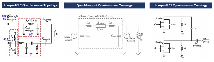
There are several potential compact Doherty combining circuits that can be leveraged to achieve an integrated PA. This includes the following (Figure 2):
- Lumped CLC quarter-wave topology [1]
- Quasi-lumped quarter-wave topology [2]
- Lumped LCL quarter-wave topology [3]
Figure 2: Compact Doherty combining circuits for integrated PA in mMIMO applications [1]-[3]. Image Link
Lumped CLC Quarter-Wave Topology
As stated earlier, the bandwidth limiting factors in Doherty PAs are the quarter-wavelength transformer, phase compensation network, and the offset line. The conventional DPA includes the offset line after the quarter-wave transformer in order to compensate for the output capacitance of the transistors and to maintain ideal output load impedance values of both amplifiers. This, however, degrades the effective bandwidth of the system as it has a narrower bandwidth than the quarter-wavelength transformer.
In one iteration of the lumped CLC quarter-wave topology, the output capacitor of the carrier amplifier is merged into the CLC quarter-wave structure while the output capacitor of the peaking amplifier is resonated out with an RF choke inductor. Figure 3 shows the input circuit (3a), output combining circuit (3b), as well as the final schematic representation of the lumped CLC broadband DPA (3c). The use of the quarter-wavelength transformer and the differently biased transistors leads to a need for a phase compensation circuit at the input of a typical DPA. In this topology, the phase compensation network is merged into an input matching circuit [1].
Figure 3: Schematic representation of the input circuit (a), output circuit (b), and entire circuit (c) for an integrated DPA with a lumped CLC quarter-wave topology [1]. Image Link
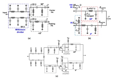
Input Matching Circuit/Phase Compensation Network
The DPA requires a class-C biased peaking amplifier that turns off in low power regions with a class-AB biased carrier amplifier for linearity in the high-power region. However, the gain of the class-C bias grows as the input power increases and because of the turn-on process of the transistor, the input capacitance increases as well, leading to a lower load impedance for the peaking amplifier. Because of this variance in the input impedance with input power level, there is a variance in the division of power between the peaking and carrier amplifiers, ultimately weakening the DPA’s broadband performance. Typically, an additional phase compensation circuit is placed at the input of the DPA to eliminate the phase difference caused by the differently-biased transistors and the addition of the quarter-wavelength transformer. Broadband input matching circuits are employed to enable a consistent division of power and input matching across the bandwidth. However, both these additions take up real-estate while the addition of the phase compensation network generally limits the bandwidth of the DPA.
It is desirable for more power to be driven to the carrier amplifier at low powers to prevent the peaking amplifier from turning on early ― an event that damages efficiency as the peaking amplifier is drawing more DC current. At high powers, it is also preferable to provide more power to the peaking amplifier in order to ensure proper load modulation and optimal linearity from IMD cancellation. A Wilkinson power divider can accomplish this load modulation by ensuring the input impedance amplifier is mismatched while the input impedance of the peaking amplifier is matched to port impedance at the maximum output power. This way, maximal power is driven to the peaking path at high powers and the effective bandwidth of the DPA is expanded. This topology includes a two-section high-pass filter (HPF) to both compensate for phase and match the input impedance with the addition of the Wilkinson divider to drive a more dynamic load modulation to maximize efficiency and linearity of the system [1][5].