
(Link to pdf for better quality graphics)
There are several reasons for the wide use of printed transmission lines. They are simple to produce, they operate over a wide bandwidth, and have small weight and dimensions.

The earliest form of printed transmission lines was the stripline (Figure 1a ).1,2 The printed stripline consists of a strip conductor centered between two parallel ground planes with two identical dielectric substrates. Small air gaps can exist between the two substrates because of fabrication faults. A dominant leaky mode that can exist in such a structure results in undesirable crosstalk and spurious performance.3 The detrimental effect of such gaps can be eliminated by using mirror image conductors (Figure 1b) on top of the bottom substrate and on the bottom of the top substrate. Due to multiple points of contact along the two conductors, the electric field in the gap is cancelled. In practice, the widths of two center conductors are purposely made slightly different (W1 ≠ W2 ). The wider conductor is given the width required for the desired characteristic impedance and the other conductor is made slightly smaller. In this way, even if the conductors are somewhat misaligned, the effective width appears constant with the proper value.
Many RF and microwave components are manufactured using suspended striplines (SS), which yield a higher Q-factor than printed stripline and microstrip lines (ML).4-7 The SS is a modified version of the stripline. In the SS (Figure 1ctoe) the strip conductors are placed on the surfaces of a thin dielectric substrate, and the substrate is then suspended in a metal enclosure. The major portion of the electromagnetic field is confined to the air gaps between dielectric substrate and ground plates. The SS propagation is purely TEM because of the uniform dielectric (air) and the symmetrical configuration. Such waves have electric and magnetic components in the plane transverse to the direction of propagation.
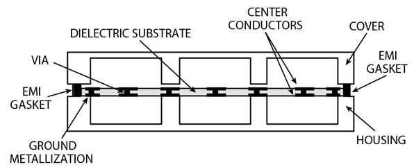
Figure 2 illustrates the cross-sectional view of a suspended stripline three-channel design. A suspended stripline circuit consists of a thin copper clad substrate, photolithographically etched, and suspended in air between identical housing and cover. This substrate is secured with internal and external walls to add further support to the PCB and provide a symmetrical position of the PCB between the housing and cover. Plated through-holes (vias) and electromagnetic interference (EMI) gaskets in the area of the support walls provide grounding connection between the housing and cover, channel-to-channel isolation, RF leakage suppression and moisture sealing. The channel dimensions should be chosen so that the spurious waveguide mode propagation is inhibited.
The suspended stripline has the following advantages:
- it provides low losses and high Q-factor (up to 500) because most of the propagated energy is in the air dielectric
- the air dielectric also helps to increase the integrated circuit dimensions which are crucial for high microwave and millimeter-wave devices, and offers larger fabrication tolerances
- the dielectric characteristics of the supported substrate have a negligible effect on the attenuation and phase velocity of the transmission medium
- a wide range of impedance values (up to 150 Ω ) is available
- it possesses good temperature stability
- with good design, it has no waveguide modes
- it operates over wide bandwidth
- there is no radiation to the outside
- both sides of the suspended substrate are available for circuit patterns enabling broadside strong coupling or combination with microstrip, coplanar or slot line
The disadvantages of the suspended striplines are difficulties in miniaturization and critical housing technology.
In the basic shielded high Q SS (Figure 1d), the parallel strips are printed on both sides of the dielectric substrate in a symmetrical configuration. The top-to-bottom circuit board interconnections are achieved via plated through-holes. This is realized by drilling a hole through the dielectric substrate and then chemically depositing electroless copper inside the walls of the hole in order to bridge the two conductors of the SS. When the dual center conductors in the SS are located symmetrically over each other, they are excited in phase, causing most of the electromagnetic field to propagate in the air dielectric. Therefore, the dielectric loss of the carrier substrate and variation in its dielectric constant have negligible effects on the attenuation and phase velocity of the transmitted waves. An added benefit of the symmetrical positioning of the conductors is that it prevents the launching of parasitic modes. The symmetrical geometry requires tight tolerances on the front-to-back etched pattern alignment and additional vias to connect these strips.
In the one-conductor SS, the transmission characteristics depend on the substrate thickness h, substrate dielectric constant, air-space height and width of the strip conductor. The characteristic impedance dependence on h occurs when the position of the dielectric substrate inside the housing is somewhat asymmetrical, such as when the spacing above the conductor is slightly smaller than that below the dielectric (HU < HL ). This asymmetrical configuration also slightly reduces the losses.
The ohmic losses in the above two suspended striplines are a concern. The RF currents become concentrated near the outer surface of the metal for an approximate skin depth d.5 This is usually referred to as the skin effect. The depth δ is the level at which the current I(t) in the conductor decreases to a value of 1/e (37 percent) of its surface value. The skin depth in a conductor is given by

where
σ = the conductivity of the conductor and the ground plane (σ = 5.813 x 10⁷ S/m for copper)
µ = the relative magnetic permeability (m = π> x 10-7 A/m for copper)
f = the frequency in hertz
In the suspended striplines, currents are concentrated in approximately three skin depths. The highest current density is in the top and bottom plated surfaces that have a lower conductivity than the main copper conductors of PCB.
While bare copper circuits can be etched to high precision, the poor corrosion properties of the metal make it undesirable for practical applications. Therefore, in a great many cases, a microwave PCB has a copper pattern covered with gold plating. Gold is not only a very good conductor but also has excellent corrosion resistance. However, when the copper-gold combination is etched, accelerated etching takes place on copper because of electromagnetic potentials, resulting in poor edge definition. An additional nickel barrier between copper and gold is used to prevent gold/copper interdiffusion. A nickel barrier thickness of 20 to 50 µinch is adequate to prevent an interdiffusion problem at temperatures as high as 150°C (solder reflow operations).
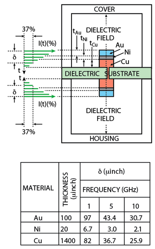
The skin depths in the three metals which form suspended stripline conductors are shown in Figure 3 . In suspended striplines at lower frequencies, the presence of a nickel plated layer can produce additional losses due to the skin effect. For instance, a 1 GHz suspended stripline circuit with a gold thickness of 50 µinch leads to a current density in the nickel of 60 percent and a current density in the gold of 40 percent. An alternative is to avoid using nickel or use a thicker gold plating (~100 µinch).
The new high Q double-substrate SS (Figure 1e)7 offers the advantage of lower ohmic losses because the microwave currents are concentrated in the high conductivity copper conductors of the PCB. This feature also expands the choice of plating material as far as its conductivity, thickness and technology process. Other advantages of this line are simple contact between the two conductors (no plated through-holes) and more integration by increasing the dielectric thickness or dielectric constant of the two substrates.
In the double-substrate SS, the widths of the two center conductors are purposely made slightly different (W1 ≠ W2 ), similar to the stripline in Figure 1b. The wider conductor is given the required width for the desired characteristic impedance, and the other conductor is made slightly smaller. In this way, even if the conductors are somewhat misaligned, the effective width appears constant with the proper value.
Some recommendations for choosing the physical dimensions of the SS follow. Large height b (the distance between top and bottom ground plates) leads to a higher power capability and Q-factor of the SS. The strip width should be decreased in order to decrease the overall dimensions, as well as to suppress the high modes. It is important to remember, however, that a smaller strip width leads to higher losses. Also, a smaller strip for the same impedance requires a smaller height. Mechanical tolerances would be more critical for a relatively small height or relatively narrow center conductors. Any vertical asymmetry in the suspended stripline structure could couple to parasitic waveguide-type modes, bounded by the ground planes and the side-walls.
Surface modes cannot propagate at frequencies for which the channel is less than a half-wavelength in width. The dimensions of the suspended stripline channel in which the substrate is supported must be sufficiently small to avoid propagation of waveguide modes. The cutoff frequency at which the TE01 mode becomes dominant is

where
a = width of the enclosure
The thickness of the dielectric substrate should be minimized for the SS in Figure 1c and d to minimize the losses and the parasitic inductance of vias, and to reduce price. For the new double-substrate SS of Figure 1e, the substrate thickness can be chosen based upon compromise between integration index and dielectric losses.
Coupled Suspended Striplines
Coupled lines are two or more transmission lines with distributed electromagnetic coupling between them. Coupled lines are a most useful and widely applied structure that provides the basis for directional couplers, filters, coupling elements and phase shifters.
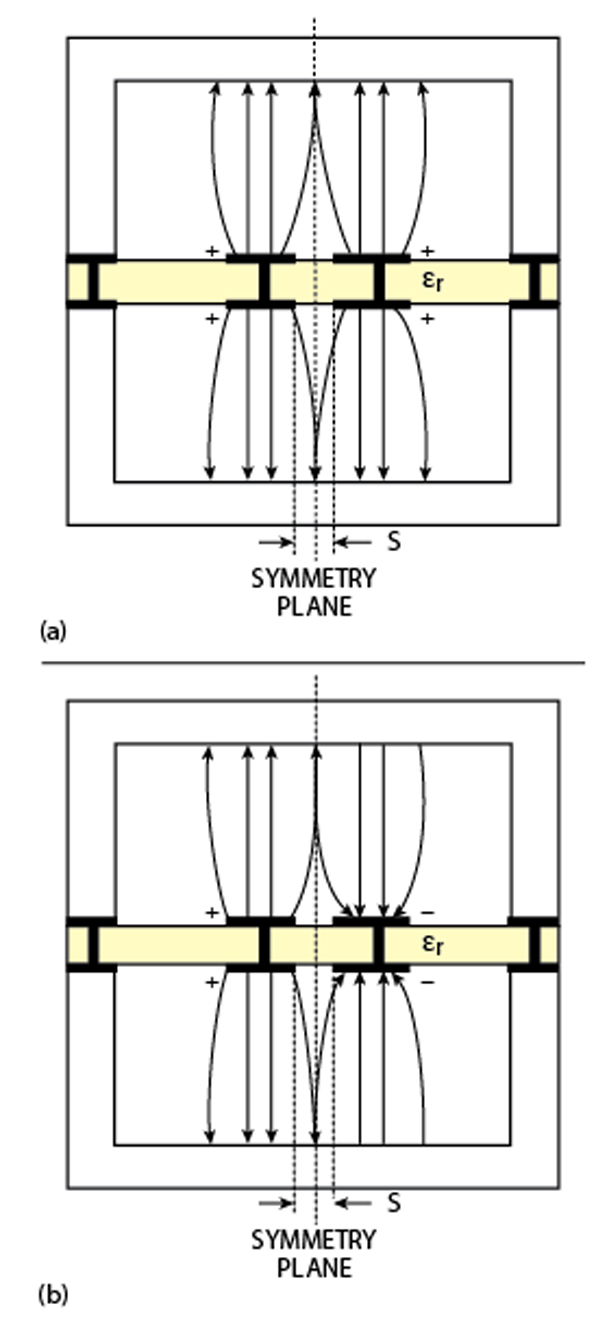
The most convenient method for calculation of coupled suspended striplines with a symmetry plane (see Figure 4 ) is the method of even- and odd-mode excitation.8-11 Then the coupled lines can be said to have even-mode and odd-mode characteristic impedances Z0e and Z0o (the last suffix identifies the mode). Z0e corresponds to the strips being at the same potential and carrying equal currents in the same direction. Z0o corresponds to the strips being at equal but opposite potentials and carrying equal currents in opposite directions. The wall at the plane of symmetry acts as an electrical wall for the odd-mode and as a magnetic wall for the even-mode.
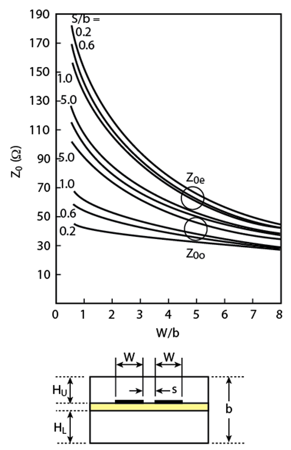
When synthesizing suspended coupled lines, the physical dimensions are determined by the even- and odd-mode impedances which are calculated based on the specified electrical characteristics of the coupled line devices (directional couplers, filters, etc). When analyzing coupled line devices, the physical dimensions are given and one must determine the electrical characteristics which depend on Z0e and Z0o . Figure 5 illustrates even- and odd-mode impedances for edge-coupled suspended striplines.
Coupled suspended striplines offer lower insertion loss and the ability to achieve tight coupling. The tight coupling is obtained for circuit patterns using broadside coupling8 (Figure 6 ).
Coupled lines are widely used in bandpass filters. Theoretically, the first spurious response of a coupled line bandpass filter occurs at three times the center frequency. In a practical microstrip parallel-coupled line bandpass filter, a spurious mode occurs at nearly twice the passband frequency because of the different even- and odd-mode propagation velocities of the coupled resonators.

In the suspended coupled striplines, electromagnetic fields propagate in an isotropic media, and the phase velocities for even- and odd-modes are equal. This property enables high performance to be achieved in filters and directional couplers. Also, coupled suspended striplines have lower losses and a lower sensitivity to fabrication tolerances than microstrip or stripline coupled lines.
Combination of Suspended Stripline and Microstrip Circuits
Suspended striplines and microstrip lines (ML) offer certain advantageous features with respect to each other.7 Although the microstrip circuit occupies a smaller area on the substrate, it has high insertion losses (lower Q-factor) and poor temperature stability. For some applications, a combination of these two types of line provides a higher performance. Both sides of the substrate are available for circuit patterns, enabling this combination. This conception is illustrated in the following examples.
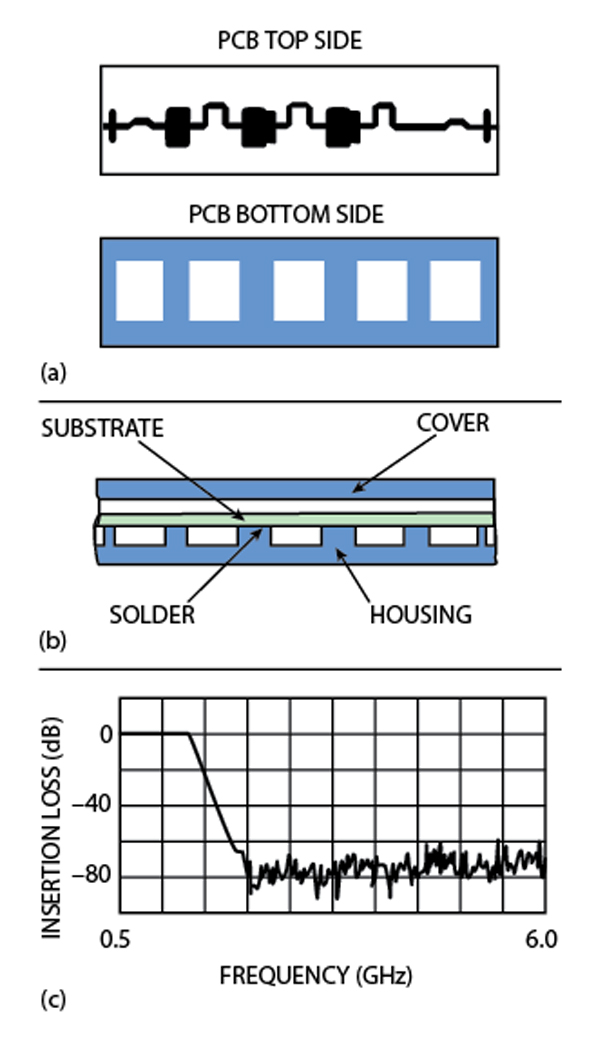
A low pass filter (LPF) that uses a combination of SS and ML is shown in Figure 7 . This design uses series high impedance suspended stripline inductive elements and low impedance shunt microstrip capacitive elements. This combination of two different lines allows a very large impedance ratio and therefore very good stopband performance in addition to small size. The capacitive element is formed with the ground plane metallization on the PCB bottom side under the low impedance line. The PCB is supported in these areas by a housing pedestal. The PCB bottom side ground plane is soldered to the housing pedestal. Inductor elements are realized by meander suspended striplines in order to minimize losses and size.
The measured insertion loss and rejection characteristics are shown for an 11-section LPF with a 10 mil Duroid™ substrate. This filter provides an insertion loss of less than 0.2 dB, an SWR of less than 1.2 in the frequency range up to 1.2 GHz, and an attenuation of more than 60 dB in the frequency range between 2 and 10 GHz.
The second example is a C-band receiver using a combination of suspended stripline and microstrip lines (Figure 8 ). To minimize the receiver input noise figure, the input circuit (BPF1 and PIN diode switch) is based on a high Q SS. The low noise amplifier (LNA) and another network are based on ML. The ML offers advantages of size reduction, heat removal and easy ground connection.
The suspended stripline BPF112 includes coupled lines and open-ended lines. The half-wavelength resonators are bent in the center and are connected with the open-ended line. The physical length of the open-ended line is equal to a quarter-wavelength at the second harmonic of the input signal for high second harmonic attenuation. The C-band suspended stripline BPF1 shows the following electrical characteristics: insertion losses are less than 0.5 dB, the 3 dB bandwidth is 5.5 percent, the 20 dB bandwidth is 17 percent and the second harmonic attenuation is greater than 40 dB.
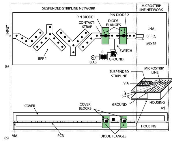
The suspended stripline, two-diode, shunt-iterated SPST switch is also shown. For PIN diodes M5X3736 (Metelics) with a junction capacitance of 0.12 pF, the optimum spacing between diodes is a little less than a quarter-wavelength (electrical length Θ<90°). The main objectives in the design of the suspended stripline switch are low insertion loss and high isolation. This C-band switch provides isolation greater than 50 dB and loss less than 0.5 dB.
The suspended stripline switch is connected to a microstrip LNA, BPF2 and a mixer. The microstrip design offers advantages for heat removal, a good ground connection and small size for the LNA and output elements. The interconnection between the suspended stripline switch output and microstrip network is shown.7 The top conductors of the SS and ML are positioned on the same side of a single dielectric substrate, and share the same top ground plate (cover). The bottom conductor of the SS has no connection with the microstrip bottom ground plate (space S), which is connected with the bottom SS ground plate (housing). Improvements in bandwidth and size minimization can be carried out by adjusting the transition line shape (gradually decreasing width) and space S. Experimental results are 0.1 dB insertion loss (max) and 19 dB return loss (min) in the C-band frequency range. This example of a combination of suspended stripline and microstrip elements is effective for simultaneously providing frequency selectivity, low noise figure and small dimensions.
References
1. R.M. Barrett, "Microwave Printed Circuits - A Historical Survey," IRE Transactions on Microwave Theory and Techniques , Vol. 3, No. 2, March 1955, pp. 1-9.
2. H.A. Wheeler, "Transmission-line Properties of a Strip Line Between Parallel Planes," IEEE Transactions on Microwave Theory and Techniques , Vol. 26, No. 11, November 1978, pp. 866-876.
3. D. Nghiem, J.T. Williams, D.R. Jackson and Q.A. Oliver, "The Effect of Substrate Anisotropy on the Dominant-mode Leakage from Stripline with an Air Gap," IEEE MTT-S International Microwave Symposium , Vol. 1, 1995, pp.141-144.
4. T. Itoh, "Overview of Quasi-planar Transmission Lines," IEEE Transactions on Microwave Theory and Techniques , Vol. 37, No. 2, February 1989, pp. 275-280.
5. I.D. Rhodes, "Suspended Substrate Filters and Multiplexers," Proceedings of 1986 European Microwave Conference , 16th EuMc, pp. 8-18.
6. V. Lander, "Designing Suspended-Stripline Passive Components," MPD Microwave Product Digest , May/June 1995.
7. L.G. Maloratsky, "Reviewing the Basics of Microstrip Lines," Microwaves & RF, March 2000, pp. 79-88.
8. P. Bhartia and P. Pramanick, "Computer-aided Design Models for Broadside-coupled Striplines and Millimeter-wave Suspended Substrate Microstrip Lines," IEEE Transactions on Microwave Theory and Techniques , Vol. 36, No. 11, November 1988.
9. H.A. Wheeler, "Transmission Line Properties of Parallel Strips Separated by a Dielectric Sheet," IEEE Transactions on Microwave Theory and Techniques , Vol. 13, No. 3, March 1965, pp. 172-185.
10. J.I. Smith, "The Even- and Odd-mode Capacitance Parameters for Coupled Lines in Suspended Substrate," IEEE Transactions on Microwave Theory and Techniques , Vol. 19, No. 5, May 1971, pp. 424-430.
11. Y.Y. Wang, et al., "Analysis and Synthesis Equations for Edge-coupled Suspended Substrate Microstrip Line," 1989 IEEE MTT-S Symposium Digest , pp. 1123-1126.
12. L.G. Maloratsky, "Improve BPF Performance with Wiggly Coupled Lines," Microwaves & RF , April 2002.