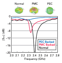
Figure 1 Effect of normal, PEC and PMC boundaries on the dipole |S11|.
A new array antenna of printed dipoles for beamforming mitigates the negative influence of nearby metal planes. This is made possible by placing a thin artificial magnetic conductor (AMC) beneath each of the printed dipole elements. Each dipole is fed by a compact bent balun suitable for connection to a Butler matrix feed network. Radiation measurements of the AMC backed dipole array demonstrate low vulnerability to a harsh environment.
Mobile communication equipment typically employs wire antennas such as monopoles or inverted L-shapes. To fit a wire antenna into a confined volume of space in an RF platform, it is a common practice to bend the radiating element close and parallel to a metallic ground, wet surface or skin (for a wearable device). In these situations, antenna input impedance matching is compromised, resulting in degraded return loss and poor radiation characteristics. This is because electromagnetic fields generated by the wire radiator in the vicinity of a perfect electrical conductor (PEC) become guided waves rather than emanating waves.1 To make the best out of the wire antenna in a handset, this drawback is circumvented with the planar inverted-F antenna (PIFA);2 however, changing the boundary condition of the metallic platform is another alternative.
The electromagnetic bandgap (EBG) structure has been adopted to mitigate the problems of a dipole near PEC or human tissue.3-8 F. Yang et al.3 placed a dipole off the edge of a pair of 4-by-3 periodic mushrooms. The PEC-backed mushroom EBG at 8 GHz reduced S11 and generated omni-directional coverage. Abkenar and Rezaei4,5 used 7-by-7 PEC-backed mushrooms over a large footprint to generate a surface wave stopband from 11 to 14 GHz. They obtain a wide-band EBG, but with no clear benefit to antenna characteristics. According to Kim et al.,6 the radiating element can be placed on the same plane as the EBG components for 7 or 8 cells of a meandered shorted-line and an interdigital gap. Shahvarpour et al.7 calculated the height of the PEC-backed multi-layered media for an AMC effect and showed 40 percent improvement in radiation efficiency for 24 GHz operation. The patches of Ayad et al.8 were modified to those of Soh et al.9 to create notches. Instead of straight dipoles, slotted patches or bent lines can be used to excite thick and wide AMCs.10-11 For these and other results reported to date, however, AMC-included antennas do not have beamforming and steering features.
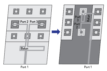
Figure 2 AMC-backed dipole comparing the conventional layout (a) with a bent balun feed (b)..
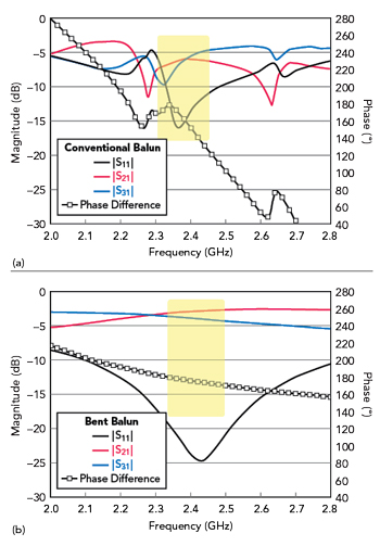
Figure 3 S-parameters vs. frequency of the conventional balun (a) and bent balun (b) structures..
In this work, we describe a thin AMC-combined array of printed dipoles connected to a Butler matrix for beamforming that is suitable for operation in harsh environments such as a close proximity to metal planes or lossy soft surfaces. To apply this method to wearable beamforming devices, 2.4 GHz is set as the operating frequency. The profile of the total structure is low, in contrast to other AMC-added antennas. It has four beams that remain nearly unchanged even in the proximity of a PEC surface. The method is verified by full-wave simulation, and by the measurement of S11 and far-field patterns.
ELEMENT AND ARRAY OF AMC BACKED DIPOLES
To demonstrate the advantages of an AMC, we conduct experiments with three different boundary conditions for a dipole antenna fabricated on FR4-substrate with a thickness of 1 mm, relative permittivity of 4.3 and tangential loss of 0.02. In Figure 1, the condition denoted as ‘normal’ (unbacked substrate) shows a sharp resonance at 2.4 GHz with an omni-directional radiation pattern. When backed by a PEC, S11 is significantly degraded as is the far-field radiation pattern. By substituting a perfect magnetic conductor (PMC) for the bottom boundary of the dipole antenna, the S11-curve and radiation pattern of the antenna are improved when in the vicinity of the PEC. To realize the PMC as an AMC, we must make an AMC that operates over the frequency band of interest.
A thin AMC-combined dipole was suggested by Khattak, and S. Kahng12 that achieves a good impedance match, adequate antenna gain and low specific absorption rate even when very close to human skin.12 This is adopted as our array antenna building block, but the geometry is improper for the planar array application, since it is fed by a coaxial cable. For the line to feed a dipole, a transmission-line balun is needed. The balun which consists of an in-phase path and an out-of-phase (180 degree) path must be carefully configured so as not to interfere with the intended characteristics of the AMC printed below the antenna.
The shape of the right-angle bent balun is compared to a conventional design in Figure 2. If the elements of the array are aligned in the lateral direction, the printed dipole should be perpendicular to the axis of the array, which makes the conventional layout inappropriate (see Figure 2a). The design is determined through optimization in an electromagnetic (EM) simulator. As shown in Figure 3, the structure divides the input RF energy equally to both the paths at the target frequency with a phase difference of 180 degrees. In contrast with the conventional balun, the bent architecture feeds the antenna elements with minimal influence on the AMC.
A more detailed view of the structure is shown in Figure 4. The printed dipole is fed by the 90 degree bent balun above the metal strip extended ground plane. The balun runs beside, without passing over, the complementary split ring resonators on the 1 mm thick FR4 substrate, leaving them undisturbed. The design is more complicated than the conventional balun because the 90 degree-bend in the main and coupled paths makes impedance matching difficult, while the small gap between the two feed lines to avoid crossing over the spirals influences the impedance matching as well. The geometrical parameters for resonance at 2.4 GHz are l1, l2, l3, l4, l5, l6, d1, d2, d3, d4, d5, d6, d7, lsub, wsub, ltot, wtot, gap, w1, and w2 equal to 10, 15, 18, 24, 12 12.2, 1, 15, 2.5, 20, 1, 5, 17.5, 83.2, 50, 240, 265, 65, 20, and 10 mm, respectively. With these physical dimensions, the element antenna provides the performance shown in Figure 5.
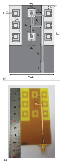
Figure 4 AMC-backed balun dipole layout (a) and fabricated antenna (b).
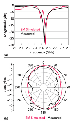
Figure 5 Element antenna |S11| (a) and E-plane far-field pattern (b).
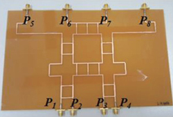
Figure 6 Fabricated Butler matrix for beamforming.
Despite the discontinuities in the balun, the impedance is matched at the targeted resonant frequency of 2.4 GHz. EM simulation and the measured results closely agree. Antenna gain is nearly 2.5 dBi with a broad beam suitable for array synthesis, although there is a slight difference between the pattern measurement results and simulation.
BUTLER MATRIX AND ANTENNA ARRAY DESIGN
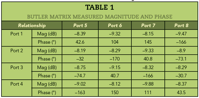
The Butler matrix is a beamforming network that is often used in beamforming antennas.13 It enables beamforming through hybrid branch line couplers, crossover networks and phase-shifters (see Figure 6). Table 1 shows the measured power distribution and phase relationships for each input port. Due to dissipation in the FR-4 substrate, losses are higher than ideal; however, the loss characteristics are uniform in each path and the phase relationships are similar to those of an ideal Butler matrix.14 The single antenna element is repeated in the lateral direction to form an array with a measured return loss less than 10 dB in the target frequency band (see Figure 7).