
 Wireless connectivity, whether for simple commercial applications such as garage door openers or for more complex military applications such as ultra-small radios, continues to be an integral part of product innovation. Embedding RF into these different applications often requires highly compact form factors and support for a wide range of frequencies. Avago Technologies’ VMMK series of amplifiers is a dramatic step in supporting this direction with micro-miniaturization of high frequency components. VMMK’s compact size and exceptional performance gives the system designer increased flexibility in meeting the demanding needs of today’s small size, high data rate RF environment. Additionally, the ability to assemble these devices using standard surface-mount techniques ensures their smooth inclusion in today’s electronic assembly line.
Challenges of Conventional Plastic Packaging
The demand for constant connectivity and smaller form factors continues to drive the need to miniaturize devices with RF functionality. Many mobile applications today demand a very thin profile that makes it extremely difficult for module manufacturers to use conventional plastic packaging. In addition, today’s high volume, high frequency plastic packaging introduces many unwanted electrical parasitics to the final product. These include dielectric parasitics due to the plastic encapsulant, transitional parasitics due to the bond wires that are needed to connect to the chip and parasitics due to the lead-frame on which the chip is mounted. This is especially harmful to wider band, higher frequency components. Attempts to change the standard packaging have resulted in solutions such as flip chip devices, where special assembly techniques are required to work with these new packages, or the use of more expensive materials to ensure proper electrical performance. The leads and associated lead-frames also limit the minimum footprint and profile that can be achieved.
WaferCap Packaging Miniaturizes RF Components
Avago has been using Chip Scale Packaging for many years to package its line of film bulk acoustic resonator (FBAR) products for use in mobile telephones. A cap wafer is essentially mounted to the device wafer through the use of a seal gasket. The result is a packaged device when the wafer is singulated. Avago has used this style of packaging to ship over a billion FBAR filters in the course of the last decade. This packaging methodology can also be applied to help solve the problem of high frequency packaging. Avago’s unique WaferCap package uses standard wafer fabrication techniques to create a completely packaged part that is equivalent in footprint to a 0402 passive component, but with a much lower profile. The final product measures 1.0 x 0.5 x 0.25 mm, providing the flexibility and performance required to fit in a wide range of RF designs. Figure 1 shows the VMMK devices.

Figure 1 Top and bottom views of the VMMK devices.
The WaferCap package is simply the electronic wafer with a cap wafer and a seal to bond the two together. This gasket provides the structural integrity that results in a part that can go through all the conventional assembly equipment used today such as chip shooters and solder reflow machines. The gasket allows WaferCap-based products to achieve a Moisture Sensitivity Level rating of 1, making them ideal for automated assembly and long-term storage. As shown in Figure 2, the gasket also allows for an air cavity to be formed between the circuit and the cap resulting in a very benign RF environment with little or no parasitics.

Figure 2 Cross-section of WaferCap chip scale packaging.
Particular attention was made to the metallurgy used on the bottom of the device so that it could be directly soldered without any change in the normal assembly process and no resulting damage to the packaged device. With WaferCap-based devices, contact is made to the chip through vias that connect the circuit board directly to the IC with no intervening bond wires. This allows for the solder pads to be entirely contained on the bottom side of the package, thus minimizing the package footprint. The 0402 package size results in a part that is 5 percent of the volume and 10 percent of the footprint of an SOT-343 package.
Introducing the WaferCap-based VMMK Family of Amplifiers
The VMMK series of amplifiers represents the first products using this revolutionary new packaging technology. These tiny amplifiers can shrink the footprint an RF device takes on a PCB by as much as 50 percent while achieving the desired support for a wide range of frequencies. VMMK amplifiers are fabricated with Avago’s industry leading enhancement mode PHEMT process and require no negative supply voltage for their operation. Table 1 shows the line-up of five amplifiers that cover the frequency range from 0.5 to 12 GHz. These amplifiers are fully matched and require very little external circuitry for full operation. Figure 3 shows the typical application circuit for these products.

Table 1 VMMK Family of Amplifiers

Figure 3 Typical application circuit for VMMK amplifiers.
The low parasitic package allows excellent broadband performance from these amplifiers. They offer excellent gain and noise figure while being matched to 50 ohms. The VMMK-2103 and the VMMK-2203 are wideband low noise amplifiers with low power consumption that can be used in diverse applications including UWB and wireless USB. The VMMK-2103 also offers a switch bypass function for optimum flexibility. The VMMK-2303 offers a choice of bias options since it can operate at a low 1.8 V and from a battery bias voltage of 3.3 V, which makes it well suited for a vast array of mobile applications. It also offers a convenient shut down feature to further minimize power consumption. Typical performance for the VMMK-2103 is shown in Figure 4.
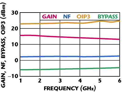
Figure 4 Gain, NF, bypass and OIP3 vs. frequency for VMMK-2103.
The VMMK-2403 and the VMMK-2503 offer higher power options with outstanding linearity levels. The VMMK-2403 features a 30 dBm output intercept point level with a 1.8 dB noise figure operating off a 3 V supply and drawing less than 40 mA. The VMMK-2403 can also be safely biased at 4 or 5 V as desired. At 3 V, the performance is an optimal compromise between power consumption, noise figure, gain and power/linearity. It can be used as a low noise block or driver. At 4 and 5 V, it draws about 48 and 62 mA, respectively. At higher Vdd, the amplifier can provide 1 to 2 dBm more output power for LO or transmitter driver applications where high output power and linearity are often required.
The VMMK-2503 is an ultra-wideband device operating from 1 to 12 GHz with a gain of 14 dB, an OIP3 of 27 dBm, a noise figure of 3.7 dB, and an excellent input and output match. Operating from a 5 V supply and drawing 65 mA, the VMMK-2503 is an outstanding multi-purpose gain block whose bias can be varied between 4 and 5 V for optimum current draw and performance. Typical performance for the VMMK-2503 is shown in Figure 5.
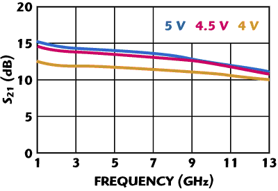
Figure 5 Typical performance for VMMK-2503
Conclusion
The VMMK series of amplifiers is the next step in ultra-miniature RF components and offers the systems designer the utmost in performance and small size. These amplifiers can be used in a wide range of RF applications, including 2.4, 3.5 and 5 to 6 GHz WLAN and WiMAX notebook computers and access points; 802.16 and 802.20 BWA systems; as well as military radar, radio and ECM systems. The 0402 footprint and the ability to assemble the devices with standard surface-mount assembly techniques give the radio designer outstanding flexibility to innovate their product designs with smaller, high-performance RF systems.
Avago Technologies,
San Jose, CA (877) 673-9442, www.avagotech.com.
RS No. 300