

The mass market for consumer wireless products led to the development of low cost packaging technology suitable for use at RF frequencies. As the market developed, there was a drive for miniaturization that helped reduce package parasitics, which assisted in pushing up the maximum operating frequency. ICs are now readily available in surface mount technology (SMT) packages with maximum operating frequencies of around 40 to 45 GHz. Further development work is now on-going to push the upper operating frequency of SMT packaged MMICs still higher. Of particular interest is SMT packaging for use at V-Band (to address the ISM bands around 60 GHz), for automotive applications at 77 and 79 GHz and for E-Band applications at 71 to 76 and 81 to 86 GHz. This article discusses the challenges of meeting these requirements and looks at the potential approaches that could be used to address them.
The most popular package style for microwave frequency ICs is the quad flat no-leads (QFN). Figure 1 shows a bare die microwave amplifier MMIC and two QFN packaged parts containing the same die type. The exposed paddle on the underside of the QFN package is normally the ground connection and is connected to the backside of the die. It is clear that the use of the bare die would still offer the ultimate in size reduction but the use of an SMT packaged component means that assembly and handling is comparatively straightforward. This facilitates reduced product cost for high volume applications and is why so much effort is being devoted to extending the frequency range of SMT packaging to still higher mm-wave frequencies.
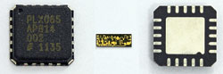
Figure 1 Microwave amplifier IC, QFN packaged and bare die.
For frequencies up to around 20 GHz, traditional over-moulded plastic packaging is normally used. In this case, the plastic moulding compound is in direct contact with the surface of the die. As operating frequencies increase, air-filled plastic cavity packages also start to be used and at still higher frequencies, laminate or liquid crystal polymer1 (LCP) based packages can be used to achieve optimum performance whilst still retaining the same QFN footprint.2
The two biggest challenges in SMT packaging of mm-wave ICs are tolerating the series inductance of the RF signal bonds and tolerating the overall grounding inductance (IC, package and PCB). With QFN packaged microwave ICs, the solid metal base provides a low grounding inductance for the package itself. The grounding inductance of the PCB, which often dominates, is minimised by:
- Using an array of ground vias providing a low inductance path from the package base to the PCB ground
- Specifying a suitably thin PCB material to reduce the inductance to the PCB ground
- Using grounded coplanar waveguide (GCPW) with close ground to signal line coupling.
The effects of package grounding are discussed in more detail in reference 3. The approach used to tolerate the series inductance of the RF bond from die to package pin is to absorb it into a lowpass filter structure.3 Provided the inductance is adequately low then the package lead-frame and PCB land pattern can be adjusted together with the bondpad on the IC to provide effective shunt capacitances of suitable values for a well-matched low loss transition.
The absolute value of the series inductance that can be absorbed into such a lowpass filter dictates the maximum frequency to which this approach can be adopted. An inductance of 0.2 nH can be absorbed into a 50 Ω matched, third order lowpass filter with a cut-off frequency of around 45 GHz and this is essentially the upper frequency limit for SMT packaging of ICs using a conventional wire-bonded approach.
To allow operation beyond 45 GHz, new packaging approaches need to be developed, which either significantly reduce or avoid the effects of series RF bond inductance and grounding inductance. The following techniques provide a means of doing this and have all been successfully demonstrated as options for SMT packaging of ICs at high mm-wave frequencies:
- Packages with waveguide (WG) apertures
- Packages with integral antennas
- Micro-coax based packaging
- Packages using ‘hot-vias’
- Flip-chip wafer level chip scale packaging (WLCSP).
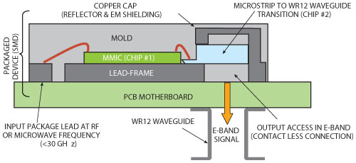
Figure 2 Formation of 77 GHz SMT package with WG aperture (courtesy of UMS).
Each of these approaches is described in more detail in the next section.
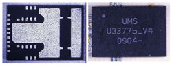
Figure 3 A plastic SMT package with integral WG aperture (courtesy of UMS).
Figure 4 A 94 GHz SMT transceiver with integral antenna array (courtesy of IBM).
Packages with WG Apertures
Various techniques exist for transforming from waveguide to microstrip or GCPW.4 The most compact approach is to use a probe transition. A probe normally extends through the broad wall of the waveguide and is positioned one quarter of a wavelength from a back-short (a waveguide short-circuit). The incoming RF signal is reflected from the back-short with a phase inversion. The reflected wave therefore adds coherently with the incident (incoming) wave at the location of the probe creating a voltage maximum. This generates an RF signal in the probe, which is passed through the broadside wall of the waveguide. Such transitions are commonly used in transceiver modules5 and, at high mm-wave frequencies, the required dimensions are such that they can be incorporated into an SMT package to provide a waveguide aperture for reception and/or transmission of the mm-wave signals.
Figure 5 A 94 GHz multi-element transceiver IC (courtesy of IBM).
Figure 2 is a cross-section of a novel SMT package to waveguide transition taken with permission from reference 6. The packaged component is a 77 GHz transmitter for automotive radar, which is mounted onto a PCB motherboard with a WR12 waveguide output on the underside. Chip #1 is the automotive radar MMIC; chip #2 is the transition realized as a printed structure on an organic PCB material.
The transition described in reference 6 demonstrates an insertion loss of 1.2 dB for a single transition at 77 GHz, based on evaluation of a back-to-back test piece. For the MMIC assembled into the WG package, the measured transmit power drops by 3 dB compared to that measured on wafer. This is mainly attributed to the wire-bonded transition from the probe substrate (chip #2) to the MMIC (chip #1) which had not yet been optimised. Both faces of the 9 × 6 mm QFN package are shown in Figure 3. Although the use of plastic packaging technology significantly reduces the cost of this style of package compared to previous ceramic versions, it is still significantly higher than conventional packaging in SMT plastic QFN packages.
Packages with Integral Antennas
Rather than attempting to develop a package with a mm-wave SMT interface, or a waveguide aperture as described previously, another alternative is to integrate the antenna into the package. Variants of this approach using both single antenna elements and multiple antenna elements (antenna arrays) have been demonstrated.7 In both cases, all other interfaces to the IC are SMT with the integral antenna forming the mm-wave transition. This approach is only possible at high mm-wave frequencies where the required physical size of the antenna becomes sufficiently small.
One of the most impressive demonstrations of this approach to date is a W-Band phased array transceiver from IBM.8 Four 16-element transceiver ICs were integrated into a single package containing 64 radiating elements. Figure 4 illustrates the package showing the antenna array. The spacing between the elements is λ/2 at 94 GHz (around 1.6 mm). The spacing from the edge antennas to the side of the package is λ/4, which facilitates the tiling of multiple components to realize a larger array. The design targets radar and active imaging applications where small size and low weight are required.
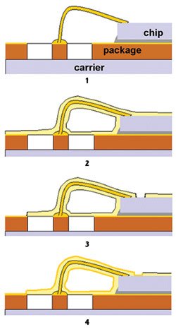
Figure 6 Formation of micro-coax interconnects (courtesy of Bridgewave).
A 16-element die is shown in Figure 5. It contains 32 receive channels (to facilitate simultaneous reception in two polarizations) and 16 transmit channels (which can be switched to either polarization). In addition to dispensing with RF bondwire inductance, the use of the multi-element antenna array has two other advantages:
- The total output power is the sum of multiple parallel transmitters so the available transmit power is increased
- The phase of the different transmit/receive elements can be adjusted to provide beam steering.
- The control of the amplitude of each transmit/receive elements also provides the possibility to shape the antenna pattern and even introduce nulls to avoid interferers.
One potential downside to this approach is that additional channel filtering cannot be included. However, the small size of the antenna means that it should provide significant rejection at low frequencies.
Micro-coax Based Packaging
Micro-coax packaging is an innovative and elegant approach to addressing the problem of RF bond inductance. The bondwire is transformed into a coaxial transmission line of controlled impedance (normally 50 Ω) by the addition of a dielectric coating and then a grounded conductive outer. Accurate control of the dielectric constant and the thickness of the dielectric are required to set the characteristic impedance of the micro-coax transmission line.
The formation of the micro-coax transition, from reference 9, is depicted in Figure 6. The package assembly steps include:
- Die attach and wire bond
- Conformal dielectric coating
- Laser cutting of vias to allow metallic contact
- Selective metallization of ground shield.
Obviously, some form of capping step would normally follow the process.
The measured performance of micro-coax test pieces has shown an insertion loss of less than 0.7 dB at frequencies up to 115 GHz for a 2.2 mm long test piece. The return loss of this test piece was better than 20 dB across most of this band with a worst case value of around 17 dB. Figure 7 is an X-ray of an 18 to 31 GHz LNA (CHA2069 from UMS) packaged using micro-coax technology. The coaxial structure of the interconnects is clearly visible, as are ground vias within the MMIC die. The measured performance of this part can be found in reference 9 and is very close to that of the bare die.
The micro-coax approach depicted in Figure 6 and Figure 7 uses a coaxial feed-through. It has the benefit that it can be used to realise a hermetically sealed package but the downside is that it is not cost-effective for most consumer applications. In order to address this, a micro-coax/leadframe approach is described in reference 9, which allows for lower production costs. A QFN style package is used as a demonstration vehicle and good performance is demonstrated to 50 GHz.
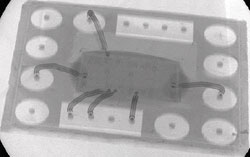
Figure 7 X-ray photograph of a micro-coax packaged LNA (courtesy of Bridgewave).
The micro-coax approach is a viable route to avoiding the effects of series RF bond inductance and as a transmission medium it has been demonstrated to show good performance to beyond 100 GHz. However, there is still some uncertainty about its potential to provide a low cost packaging solution for use in the 50 to 100 GHz range.
Packages Using Hot-Vias
Most GaAs and GaN processes include a through substrate via capability. This provides low inductance interconnects from the front side of the die to the back. The effective inductance is dependent on the substrate height and via size but is typically around 20 pH. In conventional MMIC designs, the vias are used to provide low inductance ground points with the back side of the die being ground. If patterning of the back side metal is possible, then some of these ground contacts can be isolated and can be used as low-inductance RF interconnects.
This allows the die to form the base of a true chip-scale SMT package as depicted in Figure 8. The inductance of the RF interconnect has been reduced to around 20 pH, which should, in theory, allow operation to beyond 100 GHz.
The hot-via packaging approach has previously been demonstrated10with measured through line test pieces indicating losses of 0.5 dB at 45 GHz for a single hot-via transition. The measured performance of a 15 to 30 GHz amplifier IC, modified to allow hot-via packaging, is also presented in reference 10 and shows performance similar to that of the bare die.
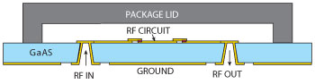
Figure 8 Use of 'hot-vias' in SMT packaging.
Avago has introduced commercially available parts in wafer scale packages (WSP) that make use of hot-vias. Published data from Avago11suggests that the hot-via transition should work well up to 45 GHz. However, at the time of writing, the product range offered in this package style does not appear to extend beyond 12 GHz.
It is clear that hot-via transitions offer a practical way to significantly reduce the series inductance of an IC to PCB transition. However, the technology has yet to prove itself practical for commercial use at mm-wave frequencies.
Flip-Chip WLCSP
In wafer level chip scale packaging (WLCSP) the die is normally packaged in a ball grid array with the surface of the die facing down towards the PCB on which it is mounted. The resulting package is truly chip scale, being not much larger than the die itself. This approach provides miniaturization and results in very low interconnect parasitics. WLCSP is often undertaken as an augmentation to the wafer fabrication process.
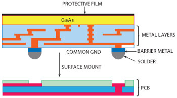
Figure 9 Cross-section of WLCSP approach (courtesy of Sumitomo).
A number of manufacturers have WLCSP processes. Infineon’s embedded Wafer Level Ball Grid Array (eWLB) technology12 has been successfully used in its V-Band and E-Band transceiver products,13 which are about to be released as commercially available products.
Sumitomo has demonstrated a set of E-Band ICs in WLCSP.14 These include a frequency tripler, an LNA, a balanced mixer and a power amplifier (PA). The packaging technology is depicted in Figure 9. The actual IC is GaAs PHEMT technology with additional processing steps to form the WLCSP. This includes the ability to add routing to connect to a uniform array of solder balls for SMT attach. The surface of the IC package is covered with a common ground metal, which has multiple links to the die ground. Openings are made in the package ground plane for signal, control and bias connections to the die.
Figure 10 shows an example of one particular WLCSP part, an LNA. The packaged part was mounted on a PCB with a GCPW interface. The performance of the packaged part on the PCB was measured with G-S-G probes, as would be used for RFOW evaluation. The comparison of the measured to modeled performance gives an honest indication of the degradation due to packaging. Each RF transition incurs an insertion loss of around 1.5 dB.
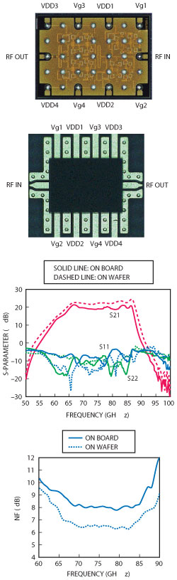
Figure 10 Example of E-Band LNA in an SMT WLCSP (courtesy of Sumitomo).
For ICs having net gain, with input and output at the same frequency (such as the LNA above), the effects of grounding inductance are much more significant than for transceivers. Great care must be taken to minimise the effective grounding inductance or severe performance degradation, or even instability, can result.
Conclusion
All of the packaging approaches described above have demonstrated their potential for use at frequencies to around 100 GHz. However, in the author’s opinion, there are two of these that are likely to see significant deployment in commercial products. These are the ICs with integrated array antennas and the flip-chip mounted ICs in WLCSP.
The integrated antennas avoid the problems associated with making a mm-wave SMT contact to a PCB. They also mean that the tolerable grounding inductance can be much higher. The use of an antenna array allows increased transmit power by in-air combination of multiple lower level signals and allows steering of the antenna beam. This approach is unlikely to be practical for longer range point to point links where higher transmit powers and antenna directivity would be required but it is very attractive for shorter range links and indoor communications.
WLCSP uses miniaturization to keep package parasitics to a minimum. The flip-chip mounting of the die means the path from the die to the PCB is minimised. The parasitics of the PCB can still have a significant effect on the ultimate performance and co-design of IC, package and PCB is necessary to achieve optimum results. With complete receiver or transmitter ICs having only a single mm-wave port, the effects of PCB grounding inductance are significantly reduced but functional blocks such as amplifiers must also tackle this issue as an integral part of their design and implementation.
Acknowledgments
The author acknowledges the valuable input from Eric Leclerc of UMS, Alberto Valdes-Garcia of IBM, Sean Cahill of Bridgewave and Miki Kubota of Sumitomo Electric Industries in the preparation of this article.
References
- S. Melvin, “Custom MMIC Packaging Solutions for High Frequency Thermally Efficient Surface Mount Applications,” Proceedings of the RF and Microwave Society (ARMMS) Conference, April 2011.
- P.W. Evans and T. Fattorini, “Electrical, Thermal, Reliability and Cost Considerations for Millimeter-Wave Surface Mount Packages,” CS MANTECH Conference, April 23-26, 2012.
- L. Devlin, “A Guide to SMT Packaging of Microwave ICs,” Proceedings of the RF and Microwave Society (ARMMS) Conference, November 19-20, 2012.
- G.A. Pearson and L.M. Devlin, “Waveguide Packaging,” Proceedings of the IEEE Colloquium on Packaging and Interconnects at Microwave and MM-Wave Frequencies, June 26, 2000, pp. 2/1-7.
- M. Piloni, G. Montiron and A.G. Milani, “E-Band Microwave Transceiver using MWgSP Technology for PtP Radio Equipment,” Proceedings of the 40th European Microwave Conference, September 2010, pp. 605-608.
- PF. Alléaume, C. Toussain, T. Huet and M. Camiade, “Millimeter-wave SMT Low Cost Plastic Packages for Automotive RADAR at 77 GHz and High Data Rate E-band Radios,” IEEE MTT-S Symposium Digest, June 2009, pp. 789-792.
- D. Liu, J. A.G. Akkermans, H.C. Chen and B. Floyd, “Packages With Integrated 60-GHz Aperture-Coupled Patch Antennas,” IEEE Transaction on Antennas and Propagation, Vol. 59, No. 10, October 2011, pp. 3607-3616.
- A. Valdes-Garcia, A. Natarajan, D. Liu et al, “A Fully-Integrated Dual-Polarization 16-Element W-band Phased-Array Transceiver in SiGe BiCMOS,” IEEE Radio Frequency Integrated Circuits Symposium, pp. 375-378, June 2013.
- K. Kuang, F. Kim and S.S. Cahill (Editors), “RF and Microwave Microelectronics Packaging, Chapter 2, November 2009, ISBN: 978-1441909831.
- A. Bessemoulin, C. Gaessler, P. Marschall and P. Quentin, “A Chip-Scale Packaged Amplifier MMIC using Broadband Hot-Via Transitions,” Proceedings of the 33rd European Microwave Conference, 2003, pp. 289-292.
- Henrik Morkner, “GaAs-Based Surface Mount Wafer Scale Package MMICs for DC to 45 GHz Application,” Avago White Paper AV02-2103EN.
- . Meyer, G. Ofner, S. Bradl, M. Brunnbauer and R. Hagen, “Embedded Wafer Level Ball Grid Array (eWLB),” Proceedings of the 10th Electronics Packaging Technology Conference, 2008, pp. 994-998.
- Infineon Technologies, “Single Chip Packaged RF Transceivers for Mobile Backhaul,” Microwave Journal, August 2013, pp. 108-110.
- K. Tsukashima, M. Kubota, A. Yonamine, T. Tokumitsu and Y. Hasegawa, “An E-Band Transmitter Module Constructed With Four WLCSP MMICs Solder - Reflowed On PCBs” Proceedings of the 7th European Microwave Integrated Circuits Conference, October 2012, pp. 207-210