
Bumping technologies for advanced semiconductor packaging have evolved significantly to address the challenges posed by shrinking contact pitches and the limitations associated with conventional flip-chip soldering. One prominent advancement in this field is the 3D Cu-Cu hybrid bonding technology, which offers a transformative solution. IDTechEx have been closely monitoring the advancements in 2.5D and 3D advanced semiconductor packaging. Their reports, titled "Advanced Semiconductor Packaging 2023-2033" and "Materials and Processing for Advanced Semiconductor Packaging 2024-2034," encapsulate their in-depth analysis and insights into the rapidly evolving landscape of 3D semiconductor packaging.
Challenges in Bump Scaling
As solder bump pitches shrink, several issues arise. Reduced bump height and surface area for bonding make it increasingly difficult to establish reliable electrical connections, necessitating precise manufacturing processes to avoid errors. Critical co-planarity and surface roughness become paramount, as even minor irregularities can compromise successful bonding.
Manufacturing faces hurdles such as etching difficulties due to smaller copper columns and bump diameters, making undercutting more likely. Electrochemical deposition (ECD) plating complexity arises as it becomes harder to effectively ensure uniformity and control co-planarity. Furthermore, the sensitivity of bonding quality to factors like bump co-planarity, surface roughness and hardness complicates adjustments to parameters like temperature, time and pressure as bump sizes continue to shrink.
Conventional flip-chip bonding methods are limited to pitches of 50 μm or 40 μm, encountering reliability issues from thermal expansion mismatches causing warpage and die shifting. To address these challenges, the semiconductor industry is transitioning to thermocompression bonding (TCB) for advanced fine pitch bonding applications, including pitches as small as 10 μm. TCB offers a promising avenue for achieving the precision and reliability required in the ever-evolving landscape of semiconductor packaging, pushing the boundaries of miniaturization and performance in electronic devices.
However, as the contact pitch reduces to around 10 microns, several issues emerge. The decreasing size of solder balls increases the risk of intermetallic compound formation, diminishing conductivity and mechanical properties. Moreover, the possibility of solder balls touching and causing bridge failures during reflow processes can lead to chip failure. These limitations become increasingly problematic in high-performance component packaging scenarios.
The Emergence of Cu-Cu Hybrid Bonding
To overcome these issues, Cu-Cu hybrid bonding technology steps in as a game-changer. This innovative technique involves embedding metal contacts between dielectric materials and using heat treatment for solid-state diffusion of copper atoms, thereby eliminating the bridging problem associated with soldering.
The advantages of hybrid bonding over flip-chip soldering are obvious. Firstly, it enables ultra-fine pitch and small contact sizes, facilitating high I/O counts. This is critical in modern semiconductor packaging, where devices require a growing number of connections to meet performance demands. Secondly, unlike flip-chip soldering, which often relies on underfill materials, Cu-Cu hybrid bonding eliminates the need for underfill, reducing parasitic capacitance, resistance and inductance, as well as thermal resistance. Lastly, the reduced thickness of the bonded connections in Cu-Cu hybrid bonding, nearly eliminating the 10 to 30 micron thickness of solder balls in flip-chip technology, opens up new possibilities for more compact and efficient semiconductor packages.
Challenges in Cu-Cu Hybrid Bonding Manufacturing
Cu-Cu hybrid bonding technology holds great promise for advanced semiconductor packaging, but it also presents a set of challenges that require innovative solutions for future development.
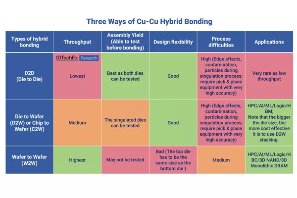
There are currently three ways of Cu-Cu hybrid bonding (see the benchmarking table below). Wafer to wafer (W2W) process is the most commonly used, whereas die-to-wafer (D2W) or chip to wafer (C2W) process is under intensive research development as it can cater to many more applications that need to integrate different sizes of dies.
For all three ways, one crucial aspect in manufacturing is the bonding environment, where achieving a flat and clean dielectric surface through chemical mechanical polishing (CMP) optimization is essential. Furthermore, the development of dielectric materials that can withstand lower annealing temperatures and shorter durations is crucial to minimize the potential for wafer distortion and warpage during the bonding process. Optimized electrochemical deposition (ECD) of copper solutions can also reduce annealing time and lower annealing temperatures, enhancing efficiency.
In the case of D2W/C2W process, addressing challenges related to die singulation and edge effects, as well as minimizing contamination on dies and wafers, will be pivotal. High accuracy pick and place machines are necessary to ensure precise die placement, with tolerances shrinking to as low as 0.2 µm. To accommodate potential placement errors, having larger Cu pads becomes imperative. Additionally, advanced thin-wafer handling technologies will play a significant role in ensuring the successful implementation of Cu-Cu hybrid bonding.
The future development of Cu-Cu hybrid bonding will likely focus on refining and optimizing these critical aspects of the process. This includes advancements in CMP, dielectric materials, ECD solutions and pick and place machinery, as well as innovations in handling thin wafers. Overcoming these challenges will pave the way for wider adoption of Cu-Cu hybrid bonding in advanced semiconductor packaging, enabling the creation of smaller, more powerful and energy-efficient electronic devices.
To learn more about 3D semiconductor packaging (Cu-Cu hybrid bonding), please refer to the IDTechEx report: "Materials and Processing for Advanced Semiconductor Packaging 2024-2034." The report is divided into four main parts, offering a structured approach to understanding advanced semiconductor packaging. The first part provides a comprehensive introduction to the technologies, development trends, key applications and ecosystem of advanced semiconductor packaging, providing readers with a solid overview of knowledge. The second part focuses on 2.5D packaging processes, delving into crucial aspects, including dielectric materials for RDL and Microvia, RDL fabrication techniques and material selection for EMC and MUF. Each sub-section within this part presents a detailed analysis of process flows, technology benchmarks, player evaluations and future trends, providing readers with comprehensive insights.
The report continues beyond the discussion of 2.5D packaging to the third part, which focuses on the innovative Cu-Cu hybrid bonding technology for 3D semiconductor packaging (Cu-Cu hybrid bonding). This section provides valuable insights into the manufacturing process and offers guidance on material selection for optimal outcomes. It also showcases case studies highlighting the successful implementation of Cu-Cu hybrid bonding using both organic and inorganic dielectrics. Additionally, the report includes a 10-year market forecast for the Organic Dielectric Advanced Semiconductor Packaging Module, presented in the last chapter. This forecast encompasses unit and area metrics, providing the industry with meaningful perspectives into anticipated market growth and trends for the next decade.