
“The advanced packaging market was worth US$30 billion in 2020 and is expected to grow at a CAGR of 8 percent to reach US$47.5 billion in 2026 during this period,” asserted Santosh Kumar principal analyst and director of Packaging, Assembly & Substrates, for Yole Développement’s activities in Korea. “At the same time, the traditional packaging market will grow at a 4.3 percent CAGR to reach US$50 billion in 2026. In this context, the total packaging market is showing a 6 percent CAGR with a US$95.4 billion value the same year.”
The advanced packaging segment is becoming more and more strategic for the semiconductor companies. According to Yole, this market is expected to more than double its revenue between 2014 and 2026.
The attractiveness of the advanced packaging is part of the economic recovery of the semiconductor industry. Therefore, after a slowdown in 2020 due to COVID-19, the global economy is set to expand by 5.6 percent in 2021, which represents its strongest post-recession pace in 80 years, and 4.3 percent in 2022. Despite the COVID-19 induced global recession, the semiconductor market performed strongly in 2020. While demand by industry was uneven throughout the year due to global lockdowns, remote work and education, online entertainment and shifts in consumer buying behavior, global semiconductor revenue grew by 6.8 percent YoY to reach US$440 billion in 2020. Going forward, the market will grow by more than 15 percent to exceed half a trillion dollars by 2022.
“Due to ongoing momentum in the advanced packaging market, the share of advanced packaging in the total semiconductor market is increasing continuously and will reach almost 50 percent of the market by 2026.” emphasized Favier Shoo, team lead analyst, Packaging at Yole. He adds: “In terms of 300 mm eq. wafer starts, traditional packaging still dominates with nearly 72 percent of the total market. However, advanced packaging is continuously increasing its share of wafers which will increase to 35 percent in 2026 to reach more than 50 million wafers. The value of advanced packaging wafer is almost double that of traditional packaging, resulting in a high profit margin for the manufacturers. Flip-chip constitutes about 80 percent of the advanced packaging market in 2020 and will continue to command a significant portion (almost 72 percent) of the market by 2026.”
Of the different advanced packaging platforms, 3D/2.5D stacking and fan-out will grow at about 22 percent and 16 percent, respectively. Adoption will continue to increase across various applications. Mainly led by mobile, Fan-In WLP (WLCSP ) will grow at a CAGR of 5 percent between 2020 and 2026. Though small (almost US$51 million in 2020), the embedded die market is expected to grow at a 22 percent CAGR in the next five years, with demand driven by the telecom and infrastructure, automotive and mobile markets.
The market research and strategy consulting company released its annual advanced packaging technology and market report, titled Status of the Advanced Packaging Industry. With this 2021 edition, analysts explore the field of advanced packaging and present a comprehensive yearly prospectus of the latest market and technology developments.
Aim of Yole’s advanced packaging team is to deliver a comprehensive analysis of the supply chain, including player positioning, market share and strategy/production per player. Moreover, this annual advanced packaging report includes revenue, wafer and unit forecasts per packaging platform across various applications, along with a review of future production and possible developments during the 2020 to 2026 timeframe.
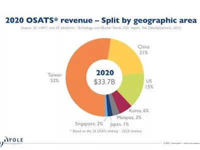
As analyzed by this new Status of the Advanced Packaging Industry 2021 report, outsourced semiconductor assembly and tests (OSATs) currently dominate the advanced packaging market. OSATs account for about 70 percent of the total market by wafer starts. However, in the high end of the packaging segment, including 2.5D/3D stacking, high-density Fan-Out, the big foundries, like TSMC and IDMs, like Intel and Samsung, dominate the market. These players are investing heavily in advanced packaging technology. This approach is strategy. Indeed, they are instrumental in moving packaging from substrate to wafer /silicon platforms.
Stefan Chitoraga, technology & market analyst at Yole commented, “TSMC earned about US$3.6 billion in advanced packaging revenue in 2020. The company announced an estimated US$2.8 billion CapEx in 2021 for its advanced packaging business specifically geared towards SoIC, SoW, and InFO variants and CoWoS product lines. In parallel, Intel’s investment in various advanced packaging portfolios, such as Foveros, EMIB, Co-EMIB, is key to implement its IDM 2.0 strategy as unveiled by new leadership. They plan to capitalize on external and internal manufacturing resources to focus on design wins and increased market share, growing Intel’s leadership in the client and data center domains.”
From its side, Samsung is aggressively investing in advanced packaging technology to boost its foundry business and emerge as a strong alternative to TSMC.
On the other hand, OSATs are also investing heavily in advanced packaging technologies to compete in the lucrative market. OSATs’ CapEx spending increased 27 percent year to year in 2020. It represents about US$6 billion. This strategy contributed to the very good financial year despite the COVID-19 impact.
Overall, there is a paradigm shift in the packaging / assembly business, traditionally the domain of OSATs and IDMs. Players from different business models including foundries, substrate/PCB suppliers, EMS/DM , are entering the assembly/ packaging business.
Supply chain shifts and implications thereof as well as the production of more than 26 major packaging suppliers per advanced packaging platform are summarized and analyzed in the report.