
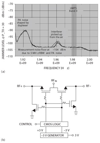
Figure 1 UltraCMOS technology-based RF switch with on-chip charge-pump negative-voltage generator (a) noise performance and (b) block diagram.
Whether in the space, military, industrial, consumer or other markets, today’s electronic designers are challenged to create low-power designs that maximize battery life while minimizing overall design size. This article will discuss how ICs built on a silicon-on-sapphire (SOS), technology process with integrated power-management functions can enable smaller, low-power RF applications.
SOS technology has long been used to minimize power consumption in many applications—from micro-power charge pumps embedded in RF switches, to integrated regulation within RF power amplifiers, to power-management/bias-control chips in transmit/receive (T/R) modules, and even DC-to-DC converter products for space applications. In addition to power consumption, another key factor that SOS technology addresses in RF applications is noise. SOS-based ICs feature an insulating sapphire substrate that provides high isolation.
As a result, it eliminates a lot of the noise issues associated with ICs that are not created in a SOS process. A specialized version of SOS ICs is UltraCMOS® technology (Peregrine Semiconductor). UltraCMOS is a technology where sapphire is the insulator. UltraCMOS technology differs from other silicon-on-insulator (SOI) technologies in that it has no conductive underlayer — meaning, this source of noise generation and coupling is eliminated. Additionally, the high level of isolation that UltraCMOS technology provides enables the integration of RF and power-management circuitry on a single chip.
Power Management in RF Products
Engineers often find it difficult to address on-chip power conversion in RFICs. For example, there may be a need for more supply voltages than one battery can provide. When the required supply voltages are greater than (or outside of) the battery rail voltages, some form of power conversion is needed. SOS technology can be used to improve power management in numerous RF devices. Examples include switches, T/R modules, and DC-to-DC converters, for end-use applications such as cellular telephones and satellite systems.
RF switches based upon SOStechnology enable higher performance, due primarily to the use of stacked low-threshold FETs on the fully-insulating sapphire substrate. These switches require a negative control voltage. If the negative voltage comes from an off-chip supply, it could lead to a power-consumption penalty in single-supply systems, and also act as a path for potential noise injection. Generating the negative voltage on-chip prevents these issues. The challenge for the switch designer, then, is to bring the negative voltage supply on chip without degrading noise performance (see Figure 1).
The RF PA in cellular phones, military radios, and portable data appliances is often the single largest power drain in the system. High-performance RF circuits are often designed with FETs that perform well at high frequencies, but are poor at turning off, and have relatively low voltage tolerance. Power-management circuitry and techniques should be employed to control the power level within the system, to ensure that the devices are not damaged by voltage extremes (such as in high VSWR and overcharge scenarios), and to maximize the circuit’s power efficiency.
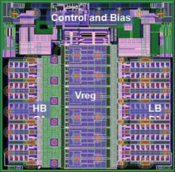
Figure 2 Dual-band RF power amplifier in CMOS-on-sapphire technology, with on-chip low dropout regulator (LDO).
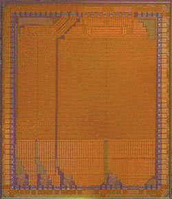
Figure 3 An UltraCMOS T/R module element control chip with four drain switches and active-bias control channels, 48-level shifting attenuator/phase shifter control I/Os and serial interface.
Dual-band constant-envelope PAs built using UltraCMOS technology typically include embedded low drop-out (LDO) regulators to optimize power-management functions (see Figure 2). The on-chip LDOs allow a 3 V CMOS technology to operate across a 2:1 battery voltage range, which allows the RF PA to remain at its ideal operating point for performance and reliability.
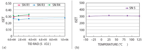
Figure 4 TX active bias set point vs. total ionizing dose (TID) (a) and vs. temperature (b).
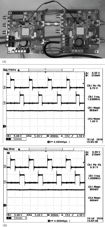
Figure 5 A 20A 2-phase DC-to-DC buck regulator (converter), using two wires (no load) (a) and 14A waveforms, 1 mV load regulation 0-14A, and a negligible voltage ripple (b).
T/R Module Power Management and Bias Control
T/R modules for space-borne radar present an unusually large power-management problem. These systems feature up to tens of thousands of radiating elements that can draw hundreds of milliamps each when active, so it is necessary to carefully control power draw. The radar performance, particularly the uniformity of element power that affects beam quality, also requires tight control of each element’s bias point across process, temperature and aging. Unfortunately, the III-V MMICs used at common radar frequencies cannot effectively throttle power by themselves. This complex set of needs can be addressed using custom UltraCMOS element-control devices for radar systems (see Figure 3).
Raw power control in T/R modules requires drain switches that handle high current and have low on resistance. For example, in systems using 3.5 V PHEMT/MHEMT technology, a single or stacked PMOS FET can handle 1 A of current at under 100 mΩ. Two- and four-channel versions are available. The drain switches incorporate fault protection via cross lockout and gate control under-voltage. This is relatively easy to achieve in an integrated approach, but it is less practical with discrete devices. In the case of the UltraCMOS technology switch, a serial control channel with numerous level-shifter outputs translates the positive CMOS control signals from the host system to the –3 V gate-control voltages required by the MMIC. The insulating sapphire substrate enables the design of a chip with four separate power domains in close proximity—CMOS VDD, TX, RX, and the –3 V VSS gate control voltage.
UltraCMOS technology can be used to integrate custom operational transconductance amplifiers (OTA) and reference ladders to accurately control bias points. Closed-loop power control maintains bias set-point accuracy across 100 Krad, and it is insensitive to supply and temperature (see Figure 4). Settling time (inclusive of drain switch turn on) is under 500 ns worst case, enabling agile radar power cycling.
The use of high-performance IC technology in space systems is limited by the availability of qualified, low-voltage power-supply solutions. In fact, the majority of available pulse-width-modulation(PWM) and linear-regulator ICs are unusable at modern low power supply voltages for a number of reasons, one having to do with maintaining stable reference voltages, and the fact that high step-down ratios are unachievable, such as those required to reduce a 40 V bus to a 1 V logic supply. However, many space systems use a 5 V rail for high-current capacity, so a distributed power approach using this resource with point-of-load (POL) converters makes sense.
POL DC-to-DC buck regulators with integrated power FETs have been designed and manufactured in UltraCMOS technology and are being used to power advanced logic devices such as SiRF FPGAs (a hardened version of Xilinx V5). Advanced FPGAs typically draw more than 10 A from a 1 V supply (as well as I/O and AUX supplies at 2.5 V), and they feature continuous current ratings of 2, 6 and 10 A that handle most applications. For higher currents, load-sharing and polyphase operation can be supported on the UltraCMOS DC-to-DC POL buck regulators using simple pin strapping (see Figure 5).
The high speed of UltraCMOS technology allows these converters to run up to 5 MHz SYNC (provided that suitable passives can be obtained) and minimizes switching losses. Figure 6 shows that peak measured efficiency is more than 92 percent at 800 KHz for a 10 A integrated POL DC-to-DC buck regulator.
The UltraCMOS-based integrated DC-to-DC POL buck regulator requires only small passive components that were deliberately left off-chip to allow easy access to set point voltage, loop dynamics, etc. (See Figure 7 and note that the power inductor is actually larger than the DC-to-DC buck regulator device.)
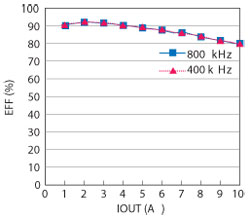
Figure 6 Measured 10A integrated POL DC-to-DC buck regulator "wallplug" efficiency vs. load current.
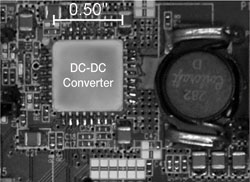
Figure 7 DC-to-DC buck regulator evaluation kit photo with scale.
Another challenge for many power-management products used in space applications is a high single-event transient amplitude and duration. These may be tolerable in a higher voltage, low/constant current application where filtering can be used to ride out the overshoot or undershoot. Modern logic ICs, however, are much more demanding in terms of DC and step currents, meaning that passive filtering alone cannot suffice. Today’s logic ICs are also much less tolerant of overstress (as little as 200 mV overshoot is outside absolute maximum ratings) and 30 percent undershoot could erase the configuration memory or at least make its contents unreliable (see Figure 8).
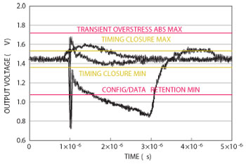
Figure 8 Linear LDO single-event transients and LV logic IC performance/reliability voltage limits, as compiled by NASA.
The UltraCMOS process is able to address issues in power hungry RF applications, and is a viable approach for systems used in space. With more than one billion RFICs shipped into a variety of markets, including space, Ultra-CMOS technology has achieved volume manufacturing, high functional density, and high-performance, high-speed operation in a variety of RF integrated circuits. Over the years, UltraCMOS has been used to integrate RF, digital, analog and power functions for commercial high-volume applications, as well as specialized high-reliability military and space products.
References
- Customer-furnished data from EVK sample.
- M.V. O’Bryan et al, “Compendium of Single Event Effects Results for Candidate Spacecraft Electronic for NASA,” IEEE NSREC 2006 W-4.