
 | |||
Due to their superior RF performance and high reliability, laterally diffused MOSFET (LDMOS) devices are widely used in high power RF amplifiers for wireless communications. For high power amplifiers, transistor reliability is always a major concern. An important characteristic that makes MOSFET devices more reliable than bipolar transistors is their negative thermal coefficient; that is, transconductance (gM) and saturated drain current (ID(sat)) decrease with increasing temperature. Unlike bipolar devices, the negative thermal coefficient prevents the device from exhibiting self-destructive thermal runaway when operating at very high power. However, the negative thermal coefficient also negatively impacts MOSFET device performance at high power. Reduced gM and ID(sat) due to self-heating decrease a device’s gain and power-handling ability.
A device’s thermal performance is best described by its thermal resistance. Clearly, the device’s power performance will be improved if thermal resistance can be lowered, as would the device reliability, since the temperature of the active area is lowered. Reduced thermal resistivity is also known to decrease a device’s memory effects and improve linearity. Infineon Technologies has been able to reduce thermal resistance by reducing the device thickness, increasing the thermal conductivity of the package, and optimizing the device layout and RF circuitry.
Lowering Thermal Resistance
A set of devices has recently been introduced using new thermally enhanced packages and die of reduced thickness. Significant thermal improvement has been observed, and a very low thermal resistance for this type of LDMOS obtained. Improvements in RF performance were also seen with higher output power and efficiency.
The 2.1 GHz, 90 W (PTF210901E) and 180 W (PTF211802E) devices are representative of these products. They use the company’s thermally enhanced package, in which the normal Cu-W flange is replaced by a composite flange. The thermal conductivity of these packages is approximately 210 to 240 W/m•K, as compared to 170 to 180 W/m•K for a Cu-W flange. In addition to the vertical path for heat dissipation, the composite material provides an enhanced heat-spreading effect that further reduces thermal resistance. Mechanically, the composite material also has an advantage over pure metal in having better stiffness.
Thermal resistance is defined as RØJC = ∆T/PD, where ∆T = TJ–TC is the temperature difference between the active junction area and package flange, and PD is the power dissipation. Using an infrared (IR) microscope, die temperature was imaged during device operations. The highest TJ on the die is used for all of the RØJC calculations. The flange was controlled at a predefined temperature (70° or 95°C) during IR scanning. Figure 1 shows a typical IR image for one die in a PTF211802E device. The device is operated at CW condition and POUT = 180 W.
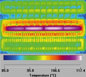 | ||
| Fig. 1 IR image showing one of four die in a PTF211802E device. | ||
Table 1 lists the results from standard Cu-W and thermally enhanced packages, under continuous wave (CW) and wideband code division multiple access (WCDMA) conditions, at both 70° and 95°C flange temperatures. It can be seen that the enhanced packages greatly reduce the thermal resistance. For the PTF211802E device, a more than 23 percent reduction in thermal resistance was observed in WCDMA conditions; the reduction in CW is as much as 28 percent. For the PTF210901E device, the reduction is shown to be between 26 and 28 percent.
 | ||
These LDMOS devices are specified to operate at TJ below 150°C. For die in a standard Cu-W package, this means the maximum package temperature TC must be about 90°C or lower when operating at rated CW power. Using a thermally enhanced package, the device is able to operate at 105°C. This will allow the devices to properly operate either inside lower cooling-budget equipment or simply in a much harsher environment.
RF Performance
Figure 2 shows the CW power response curves of PTF210901E devices in Cu-W and thermally enhanced packages. Improvements in output power and gain are clearly seen.
 | ||
| Fig. 2 PTF210901E CW power gain as a function of output power for standard Cu-W and thermally enhanced packages at 2.17 GHz. | ||
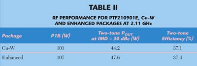
Table 2 summarizes the RF performance of devices of different packages. It can be seen that the 1 dB compression output power (P1dB) of the thermally enhanced package is about 6 percent higher. As expected, the linearity is also enhanced. The average output power, where the two-tone intermodulation distortion (IMD) equals –30 dBc, is approximately 7 percent higher; 1 MHz tone spacing has been used for these measurements. The corresponding two-tone efficiency also increases slightly.
 | ||
Conclusion
A series of RF power LDMOS devices has been introduced with the exceptional thermal performance, using a thermally enhanced package and other design optimizations. These devices have more than 23 percent reduction in thermal resistance over those using the standard Cu-W package. The significant reduction in thermal resistance allowed the devices to be used in approximately 15°C higher ambient temperature. About 6 percent more CW output power is obtained. The two-tone output power is about 7 percent higher. An improvement in efficiency is also observed.
Additional information may be obtained from the company’s Web site at www.infineon.com/rfpower.
Infineon Technologies,
RF Power Products,
Morgan Hill, CA
(408) 776-0600.