
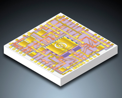
For nearly 20 years, UltraSource® has developed a sophisticated collection of thin film design solutions and modular processes that include basic single layer components for chip and wire design, integrated multilevel passives, and complex, high density, multilayer circuits. The collection of these design families and modular processes have now been organized into the UltraSource Technology Platform to provide designers with the most comprehensive suite of customizable thin film solutions available anywhere. UltraSource's Technology Platform provides designers with the opportunity to pursue innovative ideas for solving the most challenging design problems.
The platform starts with BASIC solutions consisting of conventional single and double sided 2D designs. The BASIC product family can incorporate all classic thin film substrate materials, plated through holes, sheet resistors, high conductivity traces, pre-deposited AuSn solder and solder damming options. The INTEGRATED solutions allow selection from the UltraVia, UltraBridge®, UltraCapacitor®, or UltraInductor® suite of solid state passive elements to provide higher levels of passive integration and performance. Conductor traces, resistors, capacitors, inductors, multilevel connections and filled vias can be integrated onto a single microcircuit. The MULTILAYER solution provides a five layer system that includes three layers of custom patterned gold conductors separated by two layers of polyimide dielectric. The ADVANCED solution is the ultimate in miniaturization and integrated performance. It combines the BASIC or INTEGRATED platform on one side of the device and the MULTILAYER features on the other side of the circuit. Front to back connections are made using UltraVia filled vias. These modular processes can be tailored to meet precise specifications and provide cost-effective and versatile thin film solutions.
UltraSource Inc.,
Hollis, NH
(800) 742-9410
sales@ultrasource.com
www.ultrasource.com