

This article examines how the output noise signal of RF or analog electronic components is affected by disturbances in their power supply rails, typically regulated by voltage regulator modules (VRMs). In semiconductor components, the power supply rails are connected to analog input and output ports. Consequently, any disturbance on these power rails can distort the RF or analog signals being processed. To quantify and systematically characterize this effect, the concept of power supply modulation ratio (PSMR) is often used. However, in this article, we focus on a more accessible approach, illustrating the influence of power supply variations through a series of simple and easy-to-visualize examples.
Technique for Injecting (Noise) Signal onto VRM Output
There are several excellent publications on this topic [1][2]. In this article, we adopt a similar approach with a slightly modified methodology. Specifically, we use a frequency-modulated (FM) sine wave with the following parameters:
- Center frequency: 10 kHz
- Modulation range: ±1 kHz
- Triangle frequency sweep: 100 Hz repeat rate
This FM signal is particularly useful for visualizing PSMR-related phenomena because it provides a flat peak between 9 kHz and 11 kHz under our setup. While a single-tone signal without modulation would ideally be used for precise PSMR characterization, our goal here is to illustrate the concept with accessible examples. For this purpose, the added frequency modulation enhances visualization.
Equipment
As a reference, for all experiments in this article, we have used the following equipment:
- Keysight E5052B: Source Signal Analyzer (SSA)
- Keysight 33220A: Arbitrary Waveform Generator (AWG)
- Tektronix MSO64: Oscilloscope
Experiment 1: 125 MHz Clock Source
In our first example, we examine a 125 MHz clock source. By intentionally injecting noise into the 3.3 V power supply, we expect to observe an increase in its phase noise.
This experiment targets a lower-power, higher-impedance clock generation circuit. As a result, even a small disturbance on the 3.3 V power supply can significantly affect its phase noise. This contrasts with experiment 2 (later in this article), which involves lower-impedance node manipulation.
Courtesy of Picotest, we have this VRTS3 (Voltage Regulator Test Standard, rev. 3) demo board for this experiment. The onboard 125 MHz clock source (highlighted as the green circuit block) serves as our device under test (DUT).

Preparation: Power Line Noise Injection
To supply a 3.3 V power rail to the 125 MHz clock device while superimposing our FM signal, we use a custom-modified, very low-noise, low-dropout (LDO) module. On this LDO module, the bench-top AWG signal output is connected to the noise reduction (NR) pin of the LDO. Rather than its standard noise reduction function, we repurpose the NR pin to inject a noise signal. (Note that there are many commercial "line injector" products are available in the market.)
Before measuring the 125 MHz clock DUT, we first characterize the LDO with the FM signal injection. Figure 13-1 shows the noise measurement setup for the LDO, housed inside a metal enclosure to minimize external interference.
- All components inside the metal case are battery powered, with LM317-type linear regulators used to avoid 60 Hz AC line coupling as much as possible, except AC powered E5052B.
- To inject the FM signal from the AWG into the LDO’s NR pin, we use the J2101A injection transformer.
The FM signal is isolated from the earth ground to prevent grounding issues, as the LDO output node connects to our earth-grounded analyzer. - Given the extreme low noise of the LDO, a J2181A 60 dB preamplifier is placed before the baseband port of the SSA to enhance signal detection.

Fig. 13-1 Experiment-1 Preparation Setup: 3.3V Supply LDO Measurement
From the setup shown in Figure 13-1, we obtain the 3.3 V supply profile delivered to the 125 MHz clock DUT, as illustrated in Figure 13-2. The density plot clearly highlights the 9 kHz to11 kHz FM signal superimposed on the otherwise very low-noise 3.3 V supply.
The table presents the root-mean-square (RMS) noise values for these curves.
In Figures 13-2, 13-4 and 13-5, the label "FM Noise 20 mVPP" represents the noise signal amplitude output from the AWG. The modified LDO module attenuates this signal as it passes through, reducing it from "mVPP" to "μVRMS." The 125 MHz-clock DUT ultimately receives the noise signal power from the LDO module, as quantified in the table.
(unit: μVRMS) | 10-100 kHz | 100-100 kHz | 10-10 MHz | 100-10 MHz | 10-100 MHz |
Noise Floor | 0.52 | 0.52 | 4.27 | 4.27 | 4.27 |
FM Noise OFF | 2.15 | 0.90 | 5.66 | 5.31 | 5.66 |
FM Noise 20 mVPP | 5.89 | 5.88 | 7.90 | 7.89 | 7.90 |
FM Noise 40 mVPP | 13.84 | 13.69 | 14.80 | 14.66 | 14.80 |
Table 13-1 Experiment-1 Preparation: An LDO Output RMS Noise

Fig. 13-2 Experiment-1 Preparation Plot: An LDO Output Noise Spectral Density with FM signal
Measurement Setup and Result
Now, we connect this 3.3-V LDO supply to the VRTS3 as shown in the setup of Figure 13-3, in the same metal cage.

Fig. 13-3 Experiment-1 Setup: 3.3 V LDO and VRTS3
From the setup of Figure 13-3, we obtain our phase-noise plot of the 125 MHz clock shown in Figure 13-4, which is powered by the 3.3 V supply with the FM signal of the Figure 13-2.
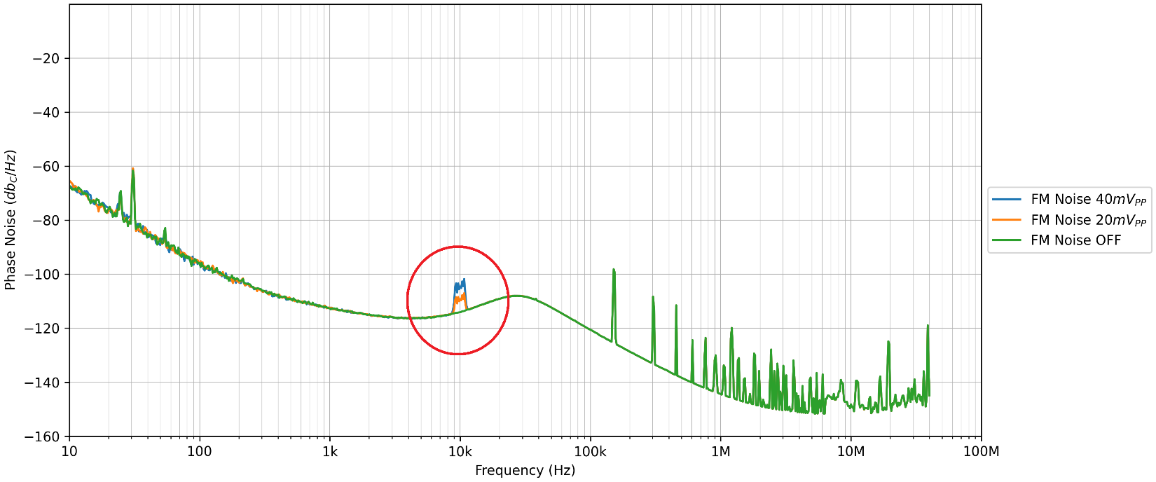
Fig. 13-4 Experiment-1 Result-1: 125 MHz Clock Phase-Noise
In Figure 13-4, we can clearly observe the blue and orange curves of 9 kHz - 11 kHz FM humps.
From Figures 13-2 and 13-4, we can exercise an interesting math manipulation: scale the datasets of Figure 13-2 overlaying to fit in Figure 13-4. After a quick trial and error, this formula makes 2 plots overlay nicely:
{Data Series into Fig. 13-4} = 20 × log10( {Data series from Fig. 13-2} ) × 0.8
Considerations
In this step, we will see the benefit of using an FM signal. In this data manipulation, our goal is to align 2 flat regions of the 9 kHz - 11 kHz. Based on the formula above, we can obtain the overlay plot seen in Figure 13-5.

Fig. 13-5 Experiment-1 Result-2: 125 MHz Clock Phase-Noise and 3.3V FM Signal
- The 125 MHz-clock DUT demonstrates high sensitivity to its power supply. From Table 13-1, even a power supply noise level in the range of 1 μVRMS is detectable on the clock output.
- The formula (again):
{Data Series into Fig. 13-4} = 20 × log10( {Data series of Fig. 13-2} ) × 0.8 - Around the 10 kHz region, the 125 MHz clock exhibits very high linearity in its sensitivity, with the 3.3 V supply noise directly influencing the clock's phase noise output.
- From Figure 13-5, we observe that an FM noise amplitude equivalent to approximately 10 mVPP becomes visible.
- Referring back to Figure 13-2, this 10 mVPP value corresponds to a noise density level of 75 nV/√Hz.
Latest Tool Preview 1
Thanks to Tektronix, we had the opportunity to test the Digital Power Management Analysis (DPM) option during experiment 1.
Using the power supply induced jitter (PSIJ) analysis tool from the DPM menu, we targeted specific frequency components where the noise of interest resides on the 125 MHz clock. The tool generates an emulated "clean" clock by effectively filtering out the identified noise frequencies. This allows us to directly compare the differences between the original clock and the emulated clean clock, providing valuable insights into the impact of power supply noise on clock performance.
Note: In this preview experiment, we observe very small but meaningful (more than error) improvement as a result of the PSIJ analysis.
Note2: For this preview, we increased the main tone frequency from 10 kHz to 100 kHz.

Fig. 13-6 Experiment 1 Preview: PSIJ Analysis
Here, we can see clearly that this PSIJ function filtered out the noise component at 100 kHz and the TIE(σ) improved from 7.884 ps to 7.308 ps.
Experiment 2: RF 1.03 GHz Low-Noise Amplifier (LNA)
Our next example is an RF 1030 MHz LNA.
We constructed a measurement setup shown in Fig. 13-7, where we have the following components.
- 5V USB-Powered Clock Synthesizer: Serves as the signal source.
- 20dB Attenuator: Reduces the signal amplitude from the source to prevent the Low-Noise Amplifier (LNA) from saturating.
- Qorvo 880367 1030 MHz IFF BAW Filter: Filters out unwanted signals from the source.
- Qorvo SGL0622Z 5 MHz to 4000 MHz, Low-Noise SiGe HBT MMIC Amplifier: Functions as the main DUT LNA.
- Battery-Powered Operation: All components are powered by batteries and housed inside a metal shielded case to minimize interference.

Fig. 13-7 Experiment-2 Setup Diagram: 1030 MHz LAN with 3.3V FM Signal
In this example, we expect to see both increasing phase noise and increasing amplitude modulation (AM) noise.
Measurement Setup and Results
In this example, we manipulate the amplifier's output stage, which involves a lower impedance node. Consequently, a stronger signal injection is required compared to experiment 1. To achieve this, we use the Picotest J2121A High Power Line Injector to introduce FM noise onto the 3.3 V supply feeding the LNA.
Figure 13-8 illustrates the measurement setup housed within the metal enclosure.

Fig. 13-8 Experiment-2 Setup: 1030 MHz LNA
To confirm the setup in Figure 13-8, we can monitor the LNA output in the time-domain using an oscilloscope as in Figure 13-9.
(In the example 1, we monitored the time-domain waveform but not shown in this article.)

Fig. 13-9 Experiment-2 Confirmation: 1030 MHz LNA Oscilloscope Waveform w/ FM Signal
- CH-1 (Yellow): Displays the LNA DUT output.
- CH-2 (Blue): Shows the 3.3 V supply with the FM signal injected from the J2121A into the LNA DUT.
- In the upper-right, full-time scale capture, we observe two things:
- The envelope of the LNA output contains the 10 kHz FM signal, highlighted in the purple rectangles.
- The 3.3 V supply shows the 10 kHz FM signal, set to 25 mVPP in this capture.
- In the lower-right zoomed waveform, we see a clean 1030 MHz sine wave with an amplitude of approximately 400 mV.
- In the right spectrum view, we observe that the LNA output contains a 10 kHz sideband signal, originating from the main 1030 MHz tone.
From Figure 13-8 setup, we can generate both the phase noise plot (Figure 13-10) and the AM noise plot (Figure 13-11).

Fig. 13-10 Experiment-2 Result-1: 1030 MHz LNA Phase Noise with FM Signal

Fig. 13-11 Experiment 2 Result 2: 1030 MHz LNA AM Noise with FM Signal
Considerations
- As expected from Figure 13-9, we observe prominent humps in the AM noise plot (Figure 13-11).
- By modulating the LNA power source, we can induce a very small phase change. Compared to Figure 13-11, the impact on phase noise in Figure 13-10 is less pronounced.
- From Figure 13-9, we can calculate the FM signal power relative to the 1030 MHz clock power using the formula:
20 × log10( 12.5 mV / 400 mV ) × 2 ≈ -60 dB - Considering the attenuation from the bypass capacitors on the SGL0622Z module, the resulting phase noise or AM noise between -80 dBC/√Hz and -100 dBC/√Hz is within the expected range.
Latest Tool Preview 2
We confirm the results of experiment 2 by taking the same measurements using two new tools.
- Courtesy of Picotest, we have a prototype of P2124A High-Speed Line Modulator.
- Courtesy of Tektronix, we have a license of Spectrum View RF versus Time Analysis.
Figure 13-12 shows updated experiment 2 setup. As you can see, Picotest P2124A simplifies the setup.

Fig. 13-12 Experiment 2 Preview: Setup with Picotest P2124A

Fig. 13-12 Experiment 2 Result 2: 1030 MHz LNA AM Noise with FM Signal
In Figure 13-12, with the new measurement option, a couple things are easier when running this evaluation.
- Spectrum-Magnitude vs. Time view shows FM signal, instead of looking at the envelope from the original time-domain waveform.
- a measurement on this spectrum-magnitude vs. time waveform, on the budge shows 8.6 kHz to 11.4 kHz of frequency-modulation (FM).
- Spectrogram shows our FM sweep.
Using this FM noise method demonstrated in experiments 1 and 2, we’ve confirmed that power supply noise does modulate onto RF or analog signal outputs.
[1] Designing Power for Sensitive Circuits, (Steve Sandler, EDI CON 2017)
[2] Measuring High Output Voltage Regulator Noise, (Masashi Nogawa and Steve Sandler, Signal Integrity Journal 2022)