
 Engineers who have only witnessed the challenges of wideband design from a distance may wonder why their peers take on such projects. After all, narrowband is more ‘comfortable’, with ample choices of low cost, high performance RF transistors. But for broadband applications such as two-way radios for first-responders, RF jammers and select radar or repeater applications, designing light-weight, highly portable end-user products is hampered by the necessity of large amplifier systems that trade efficiency performance for frequency bandwidth coverage.
In the narrowband universe, relatively high efficiency performance is possible when devices are placed in ideal impedance environments; delivering a cost-effective design approach is fairly straightforward. The broadband landscape is altogether different. Amplifiers are more difficult to design and the performance trade-offs can discourage even the most die-hard engineering intellect. Broadband high power amplifiers are typically inefficient comparatively speaking, resulting in larger, heavier systems. A wideband application by necessity often requires more elaborate cooling mechanisms and despite the best engineering efforts, exhibits inferior performance in key categories compared to narrowband counterparts.
For the design engineer who has fought the wideband battle and persevered, for those still struggling and for those who seek a better way, TriQuint has developed a solution. There’s a new discrete RF transistor that changes the equation dramatically and is already being designed into wideband systems around the globe. This new solution is called PowerBandTM (see Figure 1).

Figure 1 Block diagram illustrating how PowerBand can streamline system architecture.
Common Ground
There are several elements common to both narrowband and broadband high power amplifier designs with semiconductors, including operating voltage, class of operation and matching network considerations. Operating voltage is a key design element in high power applications. RF amplifier design becomes more difficult as the requirement for RF output power increases. This is due to several factors, but it is dominated by the inverse relationship between device size and device impedance. Later in the design process, the engineer will have to transform low impedances to higher levels via matching networks. Device impedance is primarily a factor of operating voltage, semiconductor technology and device size. As a result, designers naturally want to start with RF transistors that can function at the highest possible operating voltage since impedance matching is much easier with transistors that operate at higher voltages, such as 28 V compared to 12 V.
Class of operation is often dictated by system linearity design goals at the expense of efficiency. The RF amplifier designer therefore strives to fine tune the point in a given class of operation that maximizes efficiency while meeting linearity goals. Communications systems tend to be very focused on linearity for digital modulation schemes whereas applications such as RF jammers focus on power and efficiency.
The challenge for matching networks is to create the impedance for both the input and output of the transistor so that optimal performance can be obtained from the device. The input matching network must also allow the incoming RF signal from the stage feeding the PA to transition fully into the power amplifier stage without excessive reflection, which is also known as input return loss. Similarly, the output must provide the impedance the device requires for strong performance while also producing acceptable impedance for the circuit it feeds, such as another amplification stage, filters, switches, the antenna, etc.
In creating matching networks, designers rely on impedance and associated device performance data in the form of load-pull and source-pull tables and graphical contours provided by manufacturers. As engineers tackling these designs discover, various performance characteristics, such as gain, efficiency and output power actually require different impedances for peak performance. The designer is challenged with selecting an impedance point that provides the best overall trade-off in performance for meeting system design goals. Generally speaking, gain is sensitive to obtaining a good input match while efficiency and RF output power tend to be more sensitive to the output match.
The Challenge of Going Wide
Wideband high power RF amplifier designers must deal with all the challenges of narrowband designs while simultaneously coping with the added complexity of creating matching networks that continue to provide the RF power transistor with an acceptable impedance as the frequency changes by two octaves or more. If this wasn’t already difficult enough, many manufacturers of RF power transistors do not provide load and source-pull data across the entire useful frequency band of a given device. If the designer is fortunate enough to have an automated source and load-pull tuner system, which most do not, and is able to obtain the device impedances across the entire band of interest, they often find that the impedances required for stable, high performance operation are beyond the abilities of traditional matching networks. The problem is proportional to device capacitance, which is proportional to device size. This often leads engineers down a path of designing smaller (in terms of RF output power) amplifiers and then combining these smaller stages to achieve the desired system RF output power. This comes at a huge expense in terms of development cost, size and weight, as well as overall system costs. If the bandwidth is too great, designers resort to “channelizing” or breaking the frequency band into sections, creating amplifier stages that only target frequencies in a given range. Again, this comes with a significant financial, size and weight burden.
Advanced Semiconductors & Broadband Design
In general, high voltage compound semiconductors such as Gallium Nitride (GaN) technology have much lower capacitance per Watt of RF output power than those of other process technologies. In other words, they have higher impedances. For this reason, narrowband systems that require very high output power from a single-ended amplifier tend to turn to high voltage GaN-based power transistors. Similarly, broadband designers also take advantage of the impedance benefits of GaN because it allows them to build matching networks that operate over a greater bandwidth for a given output power level. Although more expensive than traditional technologies such as LDMOS on a per device basis, the system level cost savings of GaN are undeniable. Often, use of an advanced technology like GaN is the only reasonable solution for systems with aggressive design goals.
While advanced semiconductors like GaN have made wideband designs easier and in many cases possible, the performance is still quite low relative to what can be achieved in narrowband designs, especially in terms of efficiency. Even employing the GaN technologies now available, most current wideband designs are only able to achieve 25 to 35 percent efficiency in the final power amplifier stage.
Data that Doesn’t Fit a Wideband World
Some manufacturers market traditional RF transistors without internal matching as wideband devices. But they do not adequately characterize the transistors for use in wideband circuits. In many cases, narrowband data is published on a given device at only the high and low ends of the intended frequency range. It is much more useful to publish the “instantaneous bandwidth” RF performance, to include, at minimum, gain, efficiency and output power. Instantaneous bandwidth is commonly defined as performance for a given device in an RF fixture with bias circuitry and matching network in place so the device can be tested from one end of the frequency band to the other, with no changes being made to the circuit or device. This is different than testing a device at various frequencies in different test fixtures, each tuned to work well at a single frequency.
PowerBand Bridges the Data Divide
In contrast to traditional RF transistors, PowerBand device data sheets contain instantaneous bandwidth as well as narrowband RF performance. A table of source and load impedances is also provided along with the RF gain, efficiency and P1dB output power performance levels. In addition, a Smith chart graphic shows the optimal input and output impedance of the matching network from the low end to the high end of the band. This data is derived from placing a given device in the stated impedance environment across the entire band of operation in 100 MHz increments.
TriQuint offers narrowband data on PowerBand devices since it is useful, providing designers a sense for the degree of trade-off between wideband and narrowband performance. In addition, wideband devices are very versatile and engineers are designing them into narrowband applications for several reasons. First, wideband devices offer greater flexibility than internally matched devices, in that a single device can be used on multiple product platforms. For example, communication radio manufacturers often have several versions of a given radio that operate at different frequencies. In this case, a single PowerBand device can be used for all three radios, whereas a design employing traditional, internally matched RF transistors would require different devices for each frequency variation. In addition, designers of non-telecom systems often find it difficult to locate internally matched RF power transistors that are designed to operate in their band of interest.
A New Wideband Design Perspective
TriQuint Semiconductor approached the challenges of wideband design from an entirely new perspective that included studying the various approaches to broadband matching and impedances across a given frequency band. The goal was to create an RF power transistor that would perform well in such an impedance environment, with an emphasis on output power and efficiency. The results were dramatic: efficiency across the band (500 MHz to 3 GHz) was increased from an average of 25 to 35 percent to between 45 and 55 percent, as shown in Figure 2. This was accomplished while being able to simultaneously utilize more than 75 percent of the devices’ rated narrowband P1dB output power capability compared to a more typical usage of approximately 25 percent with traditional approaches.
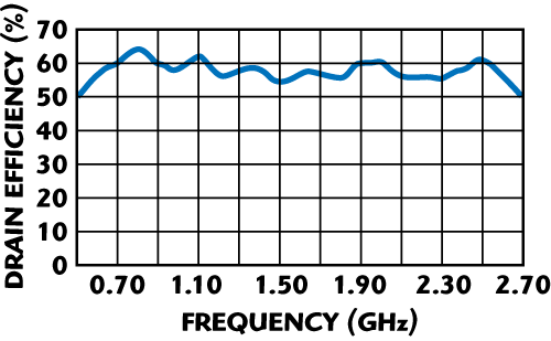
Figure 2 Measured efficiency data of a PowerBand device in a test fixture.
The PowerBand Portfolio
The TriQuint PowerBand portfolio currently consists of five products. The T1P2701012-SP is a 12 V (operating voltage) pHEMT device, operating from 500 MHz to 3 GHz; it produces 10 W P1dB (instantaneous bandwidth). The T1L2003028-SP is a 28 V (operating voltage) LDMOS-based device, operating from 500 MHz to 2 GHz and producing 30 W P1dB (instantaneous bandwidth). The T1P3002028-SP, T1P3003028-SP and T1P3005028-SP are 28 V (operating voltage), pHEMT-based products operating from 500 MHz to 2 GHz. They are designed specifically for pulsed applications and produce 20, 30 and 50 W P1dB output power (instantaneous bandwidth), respectively.
Conclusion
High power amplifier design is difficult; high power, broadband design pushes the envelope farther. Until now, performance-reducing compromises were inevitable as part of the balancing act every broadband designer was forced to perform to achieve system operating goals. While offering significantly greater bandwidth coverage and breakthrough levels of efficiency, the current PowerBand device portfolio achieves output power levels from 10 W (P1dB CW) through 50 W (P1dB pulsed). Many applications require even higher output power. The PowerBand design team recognizes this need and is at work to introduce a GaN-based portfolio in 2009 that will include a 100 W P1dB CW device (see Figure 3).

Figure 3 PowerBand 100 W GaN device under development.
TriQuint SemiconductorDesign Center,
Boulder, CO (720) 834-0017,
info-powerband@tqs.com,
www.triquint.com/powerband.
RS No. 302