Radio Frequency (RF) power amplifiers play a critical role in a broad range of wireless applications, including infrastructure for mobile devices and cell phones, broadcasting and medical equipment, satellite and military communications, emergency radios, and radar. Increasing demands on overall system performance, in turn, translates into added pressure on power amplifiers to deliver excellent efficiency (for low power consumption), linearity, and reliability at a reasonable size and cost.
As demand for cost-effective, high performance continues to mount, new and innovative techniques and materials must be introduced into the market. One such recent development is the vertical architecture being introduced with the HVVFET™ transistor from HVVi Semiconductor. The HVVFET (High Voltage Vertical Field Effect Transistor) is a discrete high power transistor for RF amplifier applications. Devices based on this new structure demonstrate excellent linearity, efficiency and high gain characteristics for high peak-to-average-ratio applications such as CDMA, WCDMA, TD-SCDMA and OFDM systems.
Higher Operating Voltage from a Vertical Device
This vertical architecture is shown in Figure 1. In contrast to lateral devices, the substrate of the HVVFET acts as the drain of the transistor. This results in a transistor capable of higher operating voltages. The HVVFET depletes vertically into the substrate as voltage is applied to the drain. This novel device architecture approaches planar breakdown in the vertical drain region, thereby standing off the maximum voltage with the minimum Rdson (on resistance). In addition to improving device packing density, the architecture greatly lowers parasitic capacitance.
The HVVFET’s unique structure provides performance characteristics that improve as the device migrates to even higher operating voltages. The company’s product roadmap is to produce greater RF power through high voltage allowing the device to operate at a lower drain-source current. This results in a smaller die size and reduced parasitic capacitance per watt. Lower capacitance supports higher-frequency operation, and the lower current density leads to improved reliability.
Efficient Heat Transfer

Heat is often the limiting factor to improving power amplifier performance. The HVVFET vertical architecture actually allows the transistors to deliver higher power while generating less heat by more efficiently removing heat from the device. Additional thermal management is achieved via a new flip-chip package expressly designed for this product. By more efficiently dissipating heat from the die, these new devices can deliver more power with higher efficiency (see Figures 2a and 2B), better gain (thereby reducing the number of amplifier stages) and improved reliability.
System Benefits
The first devices fabricated in the new HVVFET technology offer major advantages over devices built in competing technologies. In radar and avionics applications, HVVi’s new product family doubles the output power and gain in the same package footprint while reducing power consumption by 30 percent. Moreover, by lowering thermal resistance and simplifying the design, this new approach offers significant advantages in terms of ruggedness and reliability. As an example, HVVi’s initial transistors are specified to withstand a VSWR of 20:1 at all phase angles under full rated output power.
Device RF Performance
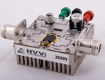
The HVVFET is currently being targeted for pulsed applications in the L-band avionics and radar markets and is available in three product families. The HVV1011-025 (30 W) and HVV1011-300 (300 W) target avionic applications such as IFF, TCAS, transponder/interrogator applications with a frequency range between 1030 and 1090 MHz (50 μsec pulse widths, 5% duty cycle). The HVV1012-050 (50 W) and HVV1012-100 (100 W) are ideal for DME avionic applications operating at 1025 to 1150 MHz and pulse widths of 10 μsec, 1% duty cycle. For ground-based radar applications, the company offers the HVV1214-025 (25 W), HVV1214-100 (100 W) and HVV1214-200 (200 W). These devices are tuned to operate in the 1200 to 1400 MHz frequency band at pulse widths of 200 μsec and 10% duty cycle. See Table 1 for performance data.

Device Packaging and Support
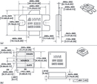
The devices come in several package types including a two-lead metal flanged HV400 package (see Figure 3a) with a liquid crystal polymer lid as well as a surface-mount transistor package with a ceramic lid (see Figure 3b). Both package styles are qualified for gross leak test—MIL-STD-750D, method 1071.6, test condition C. The 100 W and high power packaged devices also have input and output internal pre-matching to improve performance and reduce external circuit complexity.
Conclusion

This new device, the first new silicon RF power transistor structure introduced in over a decade, allows large amounts of transistor periphery to be placed in a small region of silicon, maximizing device packing density and transistor reliability while constraining the geometry of the transistor cells. The new device offers performance that is ideal for RF and microwave pulsed applications such as avionics and radar. This patent-pending vertical architecture transistor is produced in mature, proven and highly cost-effective CMOS wafer process fabrication facilities. Evaluation kits are also available.
HVVi Semiconductors Inc.
Phoenix, AZ
(480) 776-3800
www.hvvi.com
RS No. 300
