
In modern wireless communication systems, miniaturized MMIC microwave bandpass filters are required to reduce the cost and decrease the RF system design time, especially for a single RF transceiver chip. Therefore, many studies on reducing the large size of conventional bandpass filters have been made.
The lumped element approach, which uses spiral inductors and lumped capacitors, is one of the solutions to this problem. However, the design of lumped element circuits is somewhat empirical and these circuit demonstrations have been confined to frequencies up to a few gigahertz due to the low quality factors (Q)1 and low resonant frequencies of the elements.
Folded hairpin resonator filters, stepped-impedance resonator (SIR) filters2–4 and slow-wave open-loop resonator filters5 have been developed. Using these methods, a relatively compact bandpass filter can be designed. However, they still take up quite a large circuit area. Another disadvantage of these traditional microstrip filters is that they cannot effectively suppress the spurious passband, which may seriously degrade the attenuation level in the stopband and passband response symmetry, and could restrict the applicability of the filters.
Combline filters, using low temperature co-fired ceramic (LTCC) or ceramic materials with a multi-layer technology, can be used as a reduced size bandpass filter.6,7 Conventionally, however, their electrical length has been recommended to be 45° or less for efficient coupling.8 Nowadays, SAW filters are widely used in the mobile communication market. But they are still not compatible with standard IC technology and are not presently available in the frequency range up to 3 GHz.9

An active bandpass filter can be integrated in a single manufacturing process. In this case, the active circuit, which behaves as a negative resistance, is inserted10 and has a drawback associated with nonlinearity and poor noise figure.11 In this article, a novel, miniaturized, GaAs process-based MMIC filter for an RF single transceiver chip is introduced, which allows a complete module to be fabricated on a single chip, thus leading the way toward high volume components at an affordable cost.
It is composed of simple planar coupled lines shorted at their opposite ends and lumped capacitors. The main advantages of this MMIC filter are as follows: The electrical length of the resonators can be reduced to as small as a few degrees. Consequently, most chip filters using this concept can be designed to be smaller than 2 x 1 mm. Good suppression of the spurious passband is another advantage. There is no spurious up to about ten times the center frequency in this structure. This property will be most powerful as the image rejection filter in a transceiver system. Moreover, this technology is available using any kind of standard fabrication process, because the topology of this circuit is only a planar two-dimensional structure. Finally, it is also broadly applicable up to the millimeter band because the electrical length can be arbitrarily controlled. A filter, using a GaAs process technology, was designed and fabricated at 5.5 GHz to maximize the effect of the size reduction method, because a SAW filter covers only frequencies below 3 GHz and a ceramic filter is still too large to be inserted in the RF transceiver system. Simulation and measurement results are provided to verify the miniaturized GaAs bandpass filter.
Bandpass Filter Using Miniaturized λ/4 Section

In Figure 1, two artificial resonant circuits are inserted into Hirota’s circuits.12 The high impedance transmission lines with shunt lumped inductors can be replaced by coupled lines shorted at opposite ends, as shown. The two dotted networks are equivalent when the following equations are satisfied

When the miniaturized λ/4 transmission lines are connected in series, they become a typical bandpass filter, with the λ/4 section as an admittance inverter. The circuit and its equivalent circuit are shown in Figure 2. The bandwidth can be controlled by the coupling coefficient.13
Simulation and Measurement Results
First, a one-stage GaAs process bandpass filter for 5 GHz WLAN band applications, with Z0 = 50 Ω and f0 = 5.5 GHz, is designed. The electrical length of the coupled lines is set to 7°. An arbitrary Zoe can be selected and Zoo is derived. The selection of Zoe is also related to the bandwidth.
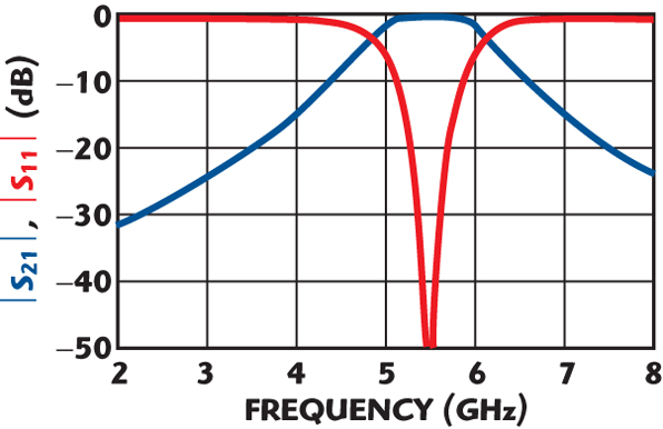
The specified response is achieved through circuit simulation with Agilent ADS and with the component values Zoe = 80 Ω, Zoo = 58 Ω and C = 3.52 pF. The physical dimensions of the coupled lines are determined by Zoe and Zoo. Figure 3 shows the calculated response of the filter, simulated with ADS. From the figure, it can be seen that the skirt characteristic is not acceptable even though the insertion loss is adequate.
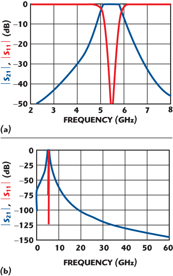
Two identical filter stages are then cascaded as a simple design. The two-stage bandpass filter behaves as a three-pole topology because an admittance inverter is formed by two resonators, one from each stage. If a conventional design technique is used, such as Butterworth or Chebyshev, the components (MIM capacitors and the coupled lines conditions) of each section are different.
In extremely miniaturized circumstances, it is very difficult to fabricate each component exactly like the designed one, because of unexpected coupling between components. Figure 4 shows the simulated ADS results. The wide band characteristic shows the good suppression of the spurious passband. Subsequently, the circuit was simulated with HFSS to obtain the overall response.
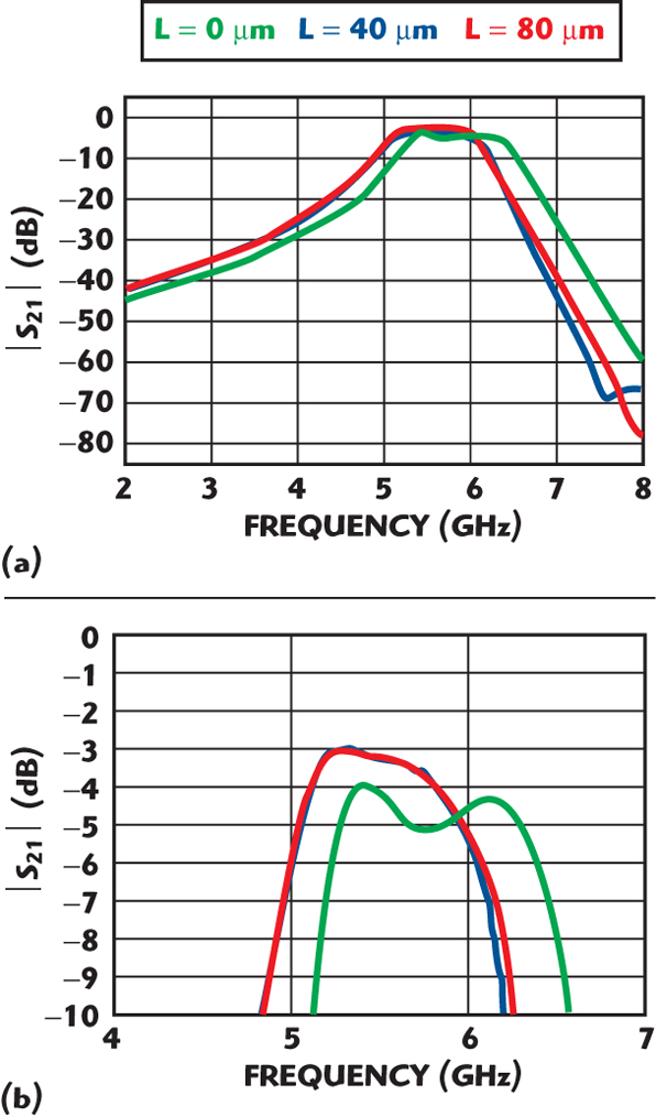
For the actual circuits, an inter-stage connecting line has been used to prevent the unexpected coupling between the two neighboring stages. In order to investigate the inter-stage line length effect on the characteristics of the filter, a group of two-stage bandpass filters with different 50 Ω inter-stage line lengths have been simulated with HFSS. Figure 5 shows the simulated results.
It can be seen that if the inter-stage transmission line is not included between two stages (L = 0 μm), a distortion appears. It is indispensable and the filtering characteristics get better as the line length increases. This concept has been explained previously.14 However, a compact size is desired, so a tradeoff between the size and good performance must be made.
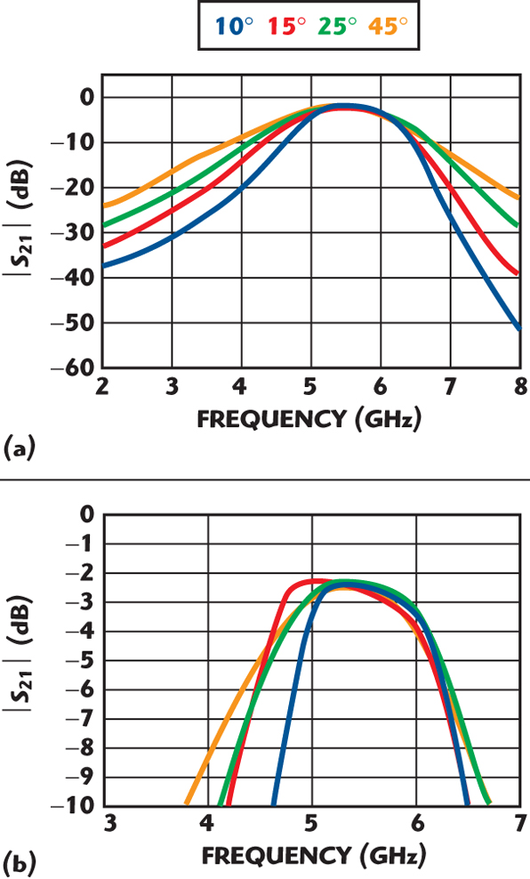
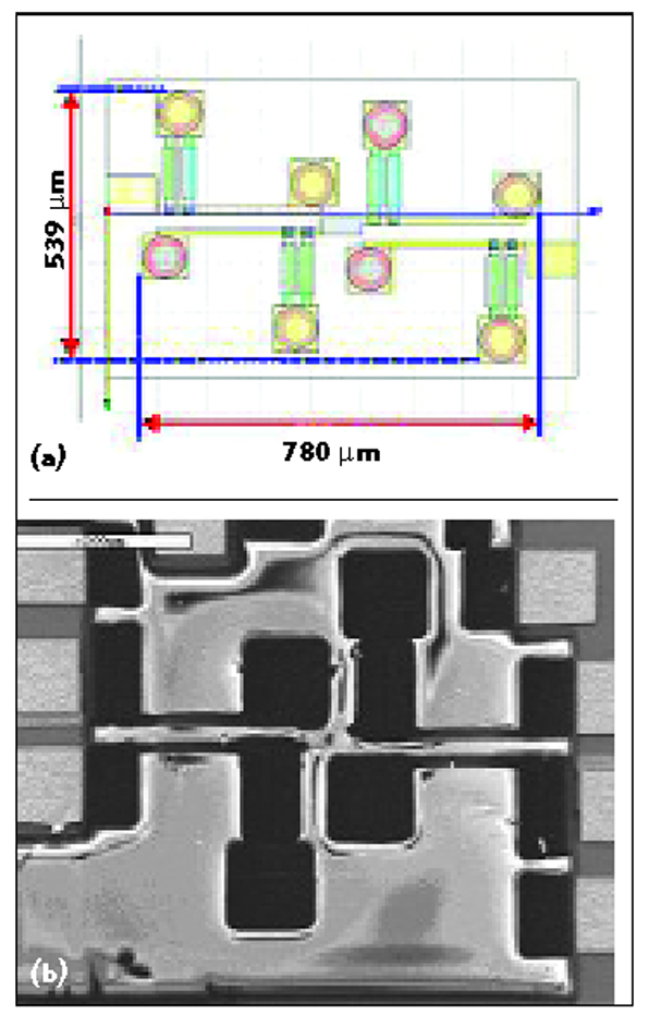
Another comparison was also made as a function of the electrical length of the coupled lines. Figure 6 shows the simulated results for 10°, 15°, 25° and 45° coupled lines filters. Obviously, the skirt characteristics of long electrical length filters are worse than that of small electrical length filters. Considering all the above-discussed factors, a two-stage bandpass filter with a 7° electrical length of coupled lines and a 80 μm long inter-stage line was designed for fabrication. Figure 7 shows the circuit layout in HFSS and the microphotograph of the MMIC. Its size is only 0.54 x 0.78 mm. As far as the authors know, this size is the most miniaturized filter for the 5 GHz WLAN band reported up until now.
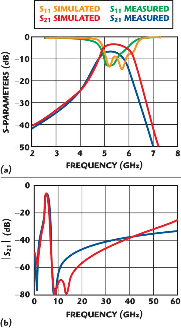
According to the HFSS simulation results shown in Figure 8, the effects of eight via holes in the filter circuit can be ignored. The figure also shows that the measured and simulated results are in good agreement. The measured passband has a maximum insertion loss of 6.5 dB over a 0.9 GHz bandwidth, from 4.8 to 5.71 GHz and a 13 dB return loss.
The measured center frequency is shifted to a lower frequency by 0.15 GHz. It is presumed to result from the MIM capacitance fabrication accuracy and simulation error. The bandwidth of measured data is shrunk from 1.15 to 0.9 GHz. Simultaneously, the insertion loss also gets worse from 3.9 to 6.5 dB. The loss error results from the HFSS simulation accuracy using a bulk conductivity of 5.8.107 Siemens/m and ignoring dielectric loss tangent of the GaAs substrate. It will be improved if the bandwidth is designed to be wider, because the wider bandwidth leads to a better insertion loss.
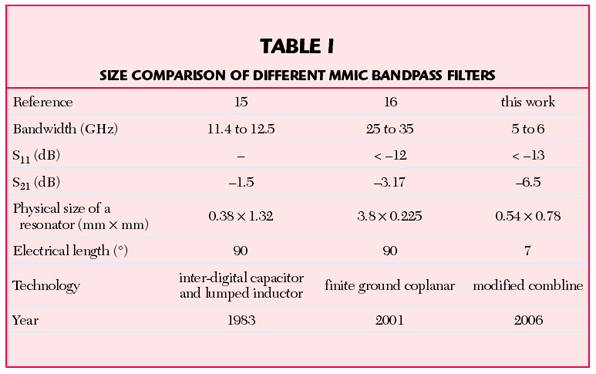
The lower band suppression is greater than 24 dB from 0 to 4 GHz and the upper band suppression is greater than 35 dB up to 60 GHz. This ultra-wide stopband characteristic is a special advantage, compared to the ceramic or SAW filters. Finally, a comparison of the sizes of different types of compact filters is made here to show the advantage of the proposed compact bandpass filter, as illustrated in Table 1.
Conclusion
A novel, miniaturized, GaAs MMIC bandpass filter, using a combination of coupled lines end-shorted at their opposite ends and lumped capacitors, was proposed in this article. Using this method, the size of the MMIC bandpass filter for an RF single transceiver chip was reduced to 0.42 mm2. This filter also has a wider upper stopband characteristic greater than 35 dB up to 60 GHz. The measured results agree well with the simulated performances. This technology can be extended to various fabrication processes because of its planar structure.
Acknowledgments
The authors wish to acknowledge Knowledge*on for its assistance and the realization of the chip. The authors also wish to express their gratitude to Joon Hwan Shim and Young Kun Seo for their support. This work was supported by the SRC/ERC program of MOST/KOSEF (Intelligent Radio Engineering Center).
References
1. B. Piernas, K. Nishikawa, T. Nakagawa and K. Araki, “Improved Three-dimensional GaAs Inductors,” 2001 IEEE MTT-S International Microwave Symposium Digest, Vol. I, pp. 189–192.
2. M. Sagawa, K. Takahashi and M. Kakimoto, “Miniaturized Hairpin Resonator Filters and Their Application to Receiver Front-end MICs,” IEEE Transactions on Microwave Theory and Techniques, Vol. 37, No. 12, December 1989, pp. 1991–1997.
3. M. Makimoto and S. Yamashita, “Bandpass Filters Using Parallel Coupled Strip-line Stepped Impedance Resonators,” IEEE Transactions on Microwave Theory and Techniques, Vol. 28, No. 12, December 1980, pp. 1413–1417.
4. A. Djaiz and T.A. Denidni, “A New Compact Microstrip Two-layer Bandpass Filter Using Aperture-coupled SIR-hairpin Resonators with Transmission Zeros,” IEEE Transactions on Microwave Theory and Techniques, Vol. 54, No. 5, May 2006, pp. 1929–1936.
5. J.S. Hong and M.J. Lancaster, “Theory and Experiment of Novel Microstrip Slow-wave Open-loop Resonator Filters,” IEEE Transactions on Microwave Theory and Techniques, Vol. 45, No. 12, December 1997, pp. 2358–2365.
6. C.W. Tang, Y.C. Lin and C.Y. Chang, “Realization of Transmission Zeros in Combline Filters Using an Auxiliary Inductively Coupled Ground Plane,” IEEE Transactions on Microwave Theory and Techniques, Vol. 51, No. 10, October 2003, pp. 2112–2118.
7. A. Kundu and N. Mellen, “Miniaturized Multilayer Bandpass Filter with Multiple Transmission Line Zeros,” 2006 IEEE MTT-S International Microwave Symposium Digest, pp. 760–763.
8. G. Matthaei, L. Young, E.M.T. Jones, Microwave Filters, Impedance-matching Networks and Coupling Structures, Artech House Inc., Norwood, MA, 1980, p. 500.
9. A. Hussain, Advanced RF Engineering for Wireless Systems and Network, John Wiley & Sons Inc., Somerset, NJ, 2005, p. 262.
10. C. Tzuang, H.H. Wu, H.S. Wu and J. Chen, “A CMOS Miniaturized C-band Active Bandpass Filter,” 2006 IEEE MTT-S International Microwave Symposium Digest, pp. 772–775.
11 J.S. Hong and M.J. Lancaster, “Microstrip Filters for RF/Microwave Applications,” Advanced Materials and Technologies, 2001, pp. 217–219.
12 T. Hirota, A. Minakawa and M. Muraguchi, “Reduced-size Branch-line and Rat-race Hybrids for Uniplanar MMICs,” IEEE Transactions on Microwave Theory and Techniques, Vol. 38, No. 3, March 1990, pp. 270–275.
13. I.H. Kang and K. Wang, “A Broadband Rat-race Ring Coupler with Tight Coupled Lines,” IEICE Communications, Vol. e88-B, No. 10, 2005, pp. 4087–4089.
14. I.H. Kang and H.Y. Xu, “An Extremely Miniaturized Microstrip Bandpass Filter,” Microwave Journal, Vol. 50, No. 5, May 2007, pp. 238–242.
15. R. Esfandiari, D.W. Maki and M. Siracusa, “Design of Integrated Capacitors and Their Application to Gallium Arsenide Monolithic Filters,” IEEE Transactions on Microwave Theory and Techniques, Vol. 31, No. 1, January 1983, pp. 57–64.
16. J. Papapolymerou and G.E. Ponchak, “Microwave Filters on a Low Resistivity Si Substrate with a Polyimide Interface Layer for Wireless Circuits,” 2001 IEEE Radio Frequency Integrated Circuits (RFIC) Symposium Digest, pp. 129–132.

In Ho Kang received his PhD degree from Sogang University, Seoul, Korea, in 1995. He is now a professor in the division of radio and information communication engineering at Korea Maritime University, Busan, Korea. His research interests include LTCC filters and MMIC filters for RF single chip for 5.5 GHz WLAN, WiMAX and UWB applications, and MMIC filters for power amplifier harmonics suppression.

Shi Wei Shan received his BS degree from the Institute of Technology at Qingdao University, China. He is now working toward his MS degree in the radio science and engineering department of Korea Maritime University. His research interests include the design, analysis, optimization and measurement of microwave circuits, including MMICs.

Xu Guang Wang received his BS degree from the department of electronics at Qingdao University, China, in 2006. He is currently working toward his MS degree in the department of radio science and engineering at Korea Maritime University, Busan, Korea.

Young Yun received his BS degree from the department of electronic engineering at Yonsei University, Seoul, Korea, in 1993. He obtained his MS degree in electrical and electronic engineering from Pohang University of Science and Technology, Pohang, Korea, in 1995, and his PhD degree in electrical engineering from Osaka University, Osaka, Japan, in 1999. From 1999 to 2003, he worked as an engineer at Matsushita Electric Industrial Co. Ltd., Osaka, Japan, where he was engaged in the research and development of MMICs for wireless communications. In 2003, he joined the department of radio science and engineering, Korea Maritime University, Busan, Korea. He is now an assistant professor, whose research interests include the design and measurement of RF/microwave and millimeter-wave ICs, and the design and fabrication of HEMTs and HBT.

Ji Hoon Kim received his BS degree in electrical engineering from Yeunngnam University, Gyeongsan, Korea, in 2001, and his MS degree in electronic engineering from the Information and Communications University (ICU), Daejeon, Korea, in 2003, where he is currently working toward his PhD degree. His research interests focus on the analysis of the nonlinearity of RF power amplifiers, linearization and efficiency improvement techniques of power amplifier MMICs for wireless handset applications.

Chul Soon Park received his BS degree in metallurgical engineering from Seoul National University, Seoul, Korea, in 1980, and his MS and PhD degrees in material science from the Korea Advanced Institute of Science and Technology (KAIST) in 1982 and 1985, respectively. Since 1999, he has been with the Information and Communications University (ICU), where he is a professor in the engineering school and director of the Intelligent Radio Engineering Center. His research interests include power amplifiers and reconfigurable RFICs and their SoC/SoP integration.