

A compact coupling structure, as the key part of a π-shaped network in the output matching impedance of a power amplifier (PA) based on the Class-EFJ mode, consists of a pair of coupling microwave lines and a sectorial microwave line. It enables the realization of the target output impedance required for Class-EFJ operation while simplifying the output matching network design. The π-shape network with this structure is used to match the fundamental impedance for the optimal fundamental design space and suppress harmonics. Relative to conventional designs, this reduces the output matching area to accommodate the need for design miniaturization while maintaining a multi-octave bandwidth. A compact multi-octave bandwidth PA is designed and fabricated for validation. The Class-EFJ PA delivers a saturated output power of 40.7 to 42.5 dBm from 0.6 to 3.3 GHz with a saturated drain efficiency of 60.7 to 72.1 percent. The PA demonstrates superior bandwidth performance compared to conventional designs.
With the rapid development of wireless communication, the amount of information transmission has increased substantially. The PA, a key transmitter module, must fulfill wide bandwidth and high efficiency requirements.1 Moreover, the wireless transceiver generally must be equipped with massive MIMO channels, e.g., 64 or 128 channels, to achieve high spectral efficiency, which challenges limitations in the circuit design area.
Therefore, it is necessary to decrease PA complexity and reduce the size of the matching circuit. Because multi-channel PAs occupy more area and require higher channel consistency, the simpler matching circuit reduces errors and increases consistency while minimizing area. Thus, the compact matching circuit has attracted greater attention.
Traditional Class-E,2,3 Class-F4,5 and Class-J6 PAs can achieve high efficiency. When mixed modes are applied, these PAs can potentially achieve wider bandwidths and higher efficiencies. Some PA output circuits consider only the output matching impedance without considering the DC bias’s impact,7 which can introduce certain errors, while simultaneously both yield greater accuracy.
Inspired by the impedance requirements of Class-EF and Class-J modes, a hybrid Class-EFJ PA with a novel π-shape compact structure is proposed here to enable multi-octave bandwidth operation. The structure is integrated into a simplified π-type output matching network, reducing the overall footprint while maintaining high efficiency across a multi-octave operating band. The size of the PA can be reduced to 45 × 56 mm. Measurement results demonstrate a saturated output power of 40.7 to 42.5 dBm from 0.6 to 3.3 GHz (a fractional bandwidth of 138 percent). Drain efficiency of 60.7 to 72.1 percent is achieved across the target frequency band.
DESIGN PHILOSOPHY
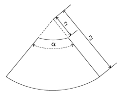
Figure 1 Sectorial microstrip line structure.
Bandwidth can be expanded by inserting a sectorial microstrip line into the bias circuit or matching circuit.8 Figure 1 illustrates the input impedance of the sectorial microstrip line, which is expressed in Equations 1 through 4:
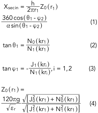
where Ji(x) and Ni(x), respectively, represent the Bessel functions of the first and second kind. The variables α, r1 and r2 are the geometric dimensions of the sectorial microstrip line (the sector angle, inner radius and outer radius, respectively). εr is the effective dielectric constant of the substrate of thickness h, and g is a constant.
To achieve the required impedance matching for the Class-EFJ PA, a novel structure is introduced (see Figure 2). It comprises a pair of coupled lines, a series microstrip line and a sectorial microstrip line, where the impedance Z1 is equal to the impedance Z2 due to symmetry. Therefore, the input impedance can be derived using even-mode and odd-mode analysis.
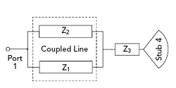
Figure 2 Coupling structure.
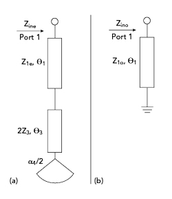
Figure 3 Even- (a) and odd- (b) mode equivalent circuits of the coupling structure.
Figure 3 shows the even- and odd-mode equivalent circuits. Even-mode and odd-mode characteristic impedances of the coupled line are denoted by Z1e and Z1o, respectively, and θ1 represents the phase angle of the coupled line. Z3 and θ3 represent the characteristic impedance and electrical phase length, respectively, of the series-connected microstrip line.
Equations 1 through 4 provide the impedance of the half-sectorial microstrip line. The coupling coefficient for a pair of microwave lines, K, is given by Equation 5:
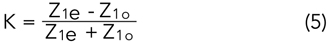
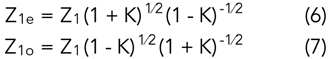
where Z1e and Z1o represent the even-mode impedance and odd-mode impedance, respectively. Thus, the coupling coefficient can be used to express the even-mode and the odd-mode characteristic impedances (see Equations 6 and 7):
The impedance transformer Z’in is given by Equation 8:
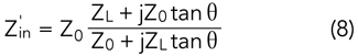
where ZL corresponds to the terminating load impedance and Z0 represents the intrinsic characteristic impedance of the microstrip line. As shown in Figure 3, Zine and Zino represent the even-mode and odd-mode input impedances, respectively. Based on Equation 8, the even-mode input impedance is given by Equation 9:
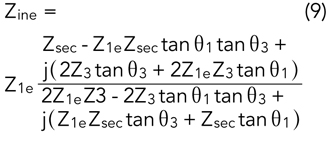
and the odd-mode input impedance is given by Equation 10:

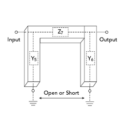
Figure 4 Two-port network circuits.
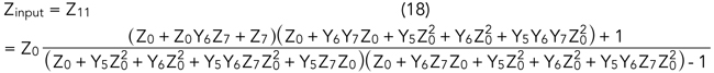
The π-shape network is shown in Figure 4. According to Li et al.,9 the parallel and series networks’ ABCD matrix is expressed by Equations 11 through 14:
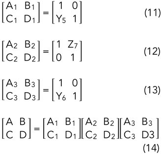
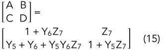
Substituting Equations 11, 12 and 13 into Equation 14 yields Equation 15:
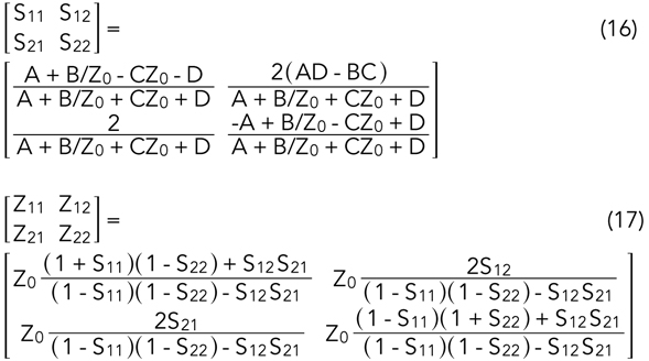
Conversion from the ABCD matrix to S- and Z-parameter matrix representations is given by Equations 16 and 17:
According to Equations 15, 16 and 17, the input impedance expression Zinput can be given by Equation 18:
A Class-EFJ PA is selected to provide a broader bandwidth. By analyzing the impedances of traditional Class-EF PAs and conventional Class-J PAs, the conditions to design hybrid Class-EFJ PAs are derived.10 The fundamental impedance is constrained within a design space defined by these conditions.