


The fundamental impedance Zfundamental is expressed in Equation 19:

where R* denotes the optimized load impedance, ranging from 15.89 to 46.29 Ω, and the coefficient γ is between -1 and 1.
To satisfy the design requirements of the Class-EFJ PA, the input impedance is within the range of 15.89 to 46.29 Ω using π-type matching networks. The optimized fundamental load impedance falls within the left half of the Smith chart.
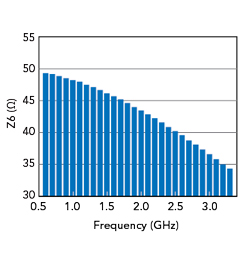
Figure 5 Simulated the Z6 (1/Y6) of the coupling structure.
From Equations 6 and 7, the coupling structure can be calculated. Impedance values of the coupling structure, 1/Y6, from 0.6 to 3.3 GHz are 34.24 to 49.37 Ω (see Figure 5). These values are transferred to the input impedance through the π-shaped network; these are also the output impedance values for the Class-EFJ PA.
The PA direct current (DC) drain bias serves as part of the output matching circuit. It replaces Y5 in the π-shaped network. The above design not only minimizes the size of the output matching circuit but also controls the second and third harmonics. This is becausethe λ/4 microwave line ensures a short circuit for the second harmonic and an open circuit for the third harmonic at the device output. This simple compact circuit provides the theoretical foundation for high efficiency and broad bandwidth.
PA DESIGN
To validate the proposed structure, a multi-octave Class-EFJ PA is designed and fabricated using a 10 W CGH40010F GaN HEMT on SiC, mounted to a Rogers 4350B circuit board (εr = 3.66, thickness = 0.762 mm). The device is biased with a drain voltage of 28 V and a gate voltage of –2.7 V. The target band is 2.7 GHz.
To ensure the accuracy of the output matching circuit, the impedance Y5 (see Figure 4) is replaced with the drain bias line in Figure 6 as a key part of the output matching circuit. The packaging parasitic parameters and π-shape network are shown in Figures 6a and 6b, respectively.11
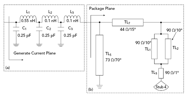
Figure 6 Transistor package model (a) and output matching network (b).
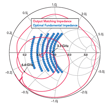
Figure 7 Output impedance at the current plane and the optimal fundamental impedance.
Figure 7 shows the fundamental load impedance presented by the output matching network at the intrinsic device plane, along with the design space for optimal fundamental impedances. The fundamental load impedance of the output matching network falls within the Class-EFJ design space. However, due to the optimization of transmission lines TL5 and TL7, the realized impedance exhibits a slight deviation from the ideal theoretical target.
The proposed structure can also improve efficiency by controlling the harmonics. The bias drain line TL5 and the series microwave line TL7 can control the second and third harmonics, as the sum of the electrical length is 85 degrees, which is approximately equal to a l/4 line. The l/4 microstrip line presents a short circuit at the second harmonic and an open circuit at the third harmonic. The electrical length of TL7, TL1 (or TL2) and the sectorial Stub 4 is about 30 degrees (λ/12), which controls the third harmonic.
The analysis demonstrates that the π-shaped output matching network with a coupling structure can effectively control fundamental and harmonic load conditions. Thus, the proposed Class-EFJ PA features a simplified design and a miniaturized layout, enhancing integration. A schematic of the PA is shown in Figure 8, and Figure 9 is a photograph of the prototype PA module. It is a compact 45 × 56 mm.
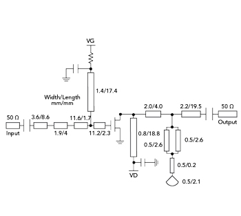
Figure 8 PA schematic.
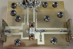
Figure 9 PA prototype.
SIMULATED AND MEASURED RESULTS
The prototype PA is driven up to 30 dBm for the measurements by CW signals at room temperature (see Figure 10). An output power of 40.7 to 42.5 dBm and a gain of 10.7 to 12.5 dB are realized from 0.6 to 3.3 GHz. Saturated drain efficiency (DE) is between 60.7 and 72.1 percent in that band as well.
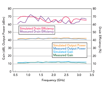
Figure 10 Simulated and measured DE, output power and gain.
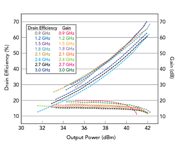
Figure 11 Measured PA linearity performance.
The measurements are consistent with the simulated values of output power and gain. Measured DE shows slight differences with the simulation over frequency, but is within the same range. The simulation model is designed with average load-pull data and other characteristics for the CGH40010F GaN HEMT family. Because the simulation model is not designed with the specific characteristics of the transistor used or test conditions, some small differences are expected.
Measured DE and gain versus output power at 0.9, 1.2, 1.5, 1.8, 2.1, 2.4, 2.7 and 3.0 GHz are shown in Figure 11. The saturated output power is 42.5 dBm at 1.8 GHz. The curves of gain versus output power are smooth, which is beneficial for linearity correction.
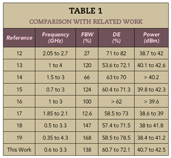
Table 1 summarizes a performance comparison with recently reported PAs. This PA achieves a significantly wider fractional bandwidth than the referenced works. The Class-EFJ PA with this proposed structure offers a well-balanced combination of high efficiency and broad bandwidth.
CONCLUSION
This Class-EFJ PA uses a π-shaped matching network in the output matching circuit. The shunt element on the output of the π-shaped network is replaced by a compact structure composed of a pair of coupled microwave lines and a sectorial microwave stub. A broadband Class-EFJ PA is designed and fabricated based on this structure, which delivers over 40.7 dBm output power with 60.7 to 72.1 percent DE across a 0.6 to 3.3 GHz frequency band.
ACKNOWLEDGMENT
This work was supported by Project of Hangzhou Dianzi University Grant Number KYS045624199, Zhejiang Provincial Science and Technology Plan Grant Number 2024C01076 and Project of Ministry of Science and Technology Grant Number: D20011.
References
- Z. Q. Cheng, Z. M. Zhao, H. J. Ke, G. Liu, Z. Dong and S. Gao, “High Efficiency Broadband GaN HEMT Power Amplifier Based on Three-Frequency Point Matching Method,” Microwave and Optical Technology Letters, Vol. 59, No. 8, May 2017, pp.1850–1855.
- F. You and J. Benedikt, “An Optimized-Load-Impedance Calculation and Mining Method Based on I-V Curves: Using Broadband Class-E Power Amplifier as Example,” IEEE Transactions on Industrial Electronics, Vol. 66, No. 7, July 2019, pp. 5254–5263.
- L. H. Zhou, X. Y. Zhou, W. S. Chan, J. Z. Pan and D. Ho, “Integrated Filtering Class-F Power Amplifier Based on Microstrip Multimode Resonator,” IEEE/MTT-S International Microwave Symposium, August 2020.
- S. Zarghami, M. Hayati, M. K. Kazimierczuk and H. Sekiya, “Continuous Class-F Power Amplifier Using Quasi-Elliptic Low-Pass Filtering Matching Network,” IEEE Transactions on Circuits and Systems II: Express Briefs, Vol. 67, No. 11, November 2020, pp. 2407–2411.
- M. Ekhteraei, M. Hayati and F. Shama, “High-Efficiency Low Voltage Inverse Class-F Power Amplifier Design Based on Harmonic Control Network Analysis,” IEEE Transactions on Circuits Systems I: Regular Papers, Vol. 67, No. 3, March 2020, pp. 806–814.
- A. Alizadeh, S. Hassanzadehyamchi and A. Medi, “Integrated Output Matching Networks for Class–J/J-1 Power Amplifiers,” IEEE Transactions on Circuits and Systems, Vol. 66, No. 8, August 2019, pp. 2921–2934.
- M. S. Jia, Z. Q. Cheng, Y. R. Shi, G. H. Liu, X. M. Zhao, H. Li and Z. W. Zhang, “Ultra-Broadband High Efficiency Class-EFJ Power Amplifier with a Compact Coupling Matching Structure,” IEICE Electronics Express, Vol. 19, No. 14, July 2022.
- S. Vardhan G., D. Pathak, M. Mendhe and A. Dutta, “15 W Hybrid GaN Power Amplifier through Microstrip Radial Stub 4W GaN MMIC for X-band Radar Applications,” IEEE VLSI Device Circuit and System Conference, July 2020.
- Y. Li, X. Fang, A. Jundi, H. Huang and S. Boumaiza, “Two-Port Network Theory-Based Design Method for Broadband Class J Doherty Amplifiers,” IEEE Access, Vol. 7, April 2019, pp. 51028–51038.
- Z. W. Zhang, Z. Q. Cheng, H. J. Ke, G. H. Liu and S. Q. Li, “Design of a Broadband High-Efficiency Hybrid Class-EFJ Power Amplifier,” IEEE Microwave and Wireless Components Letters, Vol. 30, No. 4, April 2020, pp. 407–409.
- P. J. Tasker and J. Benedikt, “Waveform Inspired Models and the Harmonic Balance Emulator,” IEEE Microwave Magazine, Vol. 12, No. 2, April 2011, pp. 38–54.
- B. Q. Zhong, Z. Q. Cheng, M. S. Jia, B. X. Li, K. Wang, Z. H. Yang and Z. M. Zhu, “Design of Bandpass Filtering Power Amplifier Based on Coupled Microstrip Line Structure,” IEICE Transactions on Electronics, Vol. E108-C, No. 5, May 2025, pp. 237–244.
- S. W. Zhao, Z. Q. Zhang, L. F. Zhou, L. S. Li and F. Zhao, “Design of a Hybrid Continuous Mode Broadband High Efficiency Power Amplifier Based on Reconfigurable Devices,” Microwave and Optical Technology Letters, Vol. 66, No. 2, February 2024.
- J. Y. Luo, Z. W. Zhang, X. F. Xuan and C. Gu, “Design of a Broadband High-Efficiency Power Amplifier Based on Continuous Class-EF Mode,” IEICE Electronics Express, Vol. 21, No. 6, February 2024.
- L. Y. Zhang, Z. W. Zhang, D. F. Zhou, C. L. Wang and C. Gu, “Design of a Broadband High-Efficiency Power Amplifier Based on a Miniaturized Three-Coupled Line Structure,” International Journal Circuit Theory and Applications, Vol. 53, No. 9, September 2025, pp. 5171–5179.
- X. He, J. S. Dong, Y. M. Yang, X. Xu and X. Q. Lin, “Design of a Broadband High-Efficiency Extended Resistive Continuous Class-B/J Power Amplifier with Novel Drain Voltage Waveforms,” Microwave and Optical Technology Letters, Vol. 66, No. 2, February 2024.
- S. B. Li, Y. L. Wu, Y. H. Yang, X. P. Chen, W. M. Wang and Z. Y. Chen, “Bandpass Filtering Power Amplifier with Wide Stopband and High Out-of-Band Rejection,” IEEE Transactions on Circuits and Systems II, Express Briefs, Vol. 70, No. 3, March 2023, pp. 969–973.
- S. Xu, J. F. Wu and X. Chen, “Design of Wideband High-Efficiency Power Amplifier Based on Microstrip Filter Matching Network with Hybrid Rings,” Microelectronics Journal, Vol. 158, April 2025.
- X. F. Xuan, Z. Q. Cheng, Z. W. Zhang and T. W. Gong, “Design an Ultra-Wideband Extended Continuous Inverse Class-GF Power Amplifiers with Source-Harmonic-Controlled Based on Rectangular Ring-Resonant Microstrip Impedance Matching Circuit,” Microelectronics Journal, Vol. 163, September 2025.