
A dozen years ago, it crossed my mind that Winslow Homer’s dramatic (some would say melodramatic) painting, “The Gulf Stream” (see Figure 1), was a nearly perfect metaphor for the microwave industry.

The ship of microwave industry is foundering in the turbulent, tropical water, afloat but with the mast snapped off and rudder missing; the poor engineer is still supported by that industry, but it is unclear how long that will continue; the sharks of unemployment are circling; the only hope of rescue, wireless technology, is almost invisible in the distance; and, finally, the economic waterspout, which caused all the damage, is leaning ominously toward that rescuer.
Was there any hope? Indeed, there was. Wireless technology has taken hold more strongly than most of us would have predicted, and has replaced a lot of volatile military business with more stable commercial business, motivated by a genuine demand from the public instead of the mercurial interests of politicians. Still, that technology has presented challenges that are startlingly difficult to meet, and they have changed the face of amplifier and oscillator design dramatically. Many of us, accustomed to heavily funded, ultra-high tech aerospace industries, were tempted to think that commercial electronic design would not be particularly challenging. Those of us beset by that illusion have been humbled, indeed.
I thought it might be fun to look at some of these technologies and see how they have affected amplifier and oscillator design, how they have created new demands, and how well those demands are being met. As it happens, I think we are doing pretty well. Certainly, challenges remain, and most of us would not have it any other way. This is one of those times when it is genuinely fun to be an engineer.
Power Amplifiers
Nowhere has the microwave landscape been changed more profoundly than in the area of power amplifier (PA) design. Not long ago, a solid-state PA with approximately 45 percent efficiency was considered quite a nice thing to have, even for such traditional high efficiency applications as spacecraft. Today, even for high linearity applications, that efficiency is marginal, and for applications where linearity is not needed (such as GSM cellular handsets), totally unacceptable. Efficiency alone is rarely enough; other requirements, such as size, cost and distortion, have assumed equal importance.
Power
Power really is not the problem. We can build amplifiers that provide any reasonable (or maybe even unreasonable) level of power that a user decides he must have. The real problem is to generate the required power consistent with all the other requirements placed upon the poor, suffering little PA chip. The most difficult of these are efficiency and linearity, directly opposing tradeoffs.
Efficiency
Obviously battery-powered equipment, such as cell phones and wireless network cards in laptop computers, must be efficient. The need for high efficiency is not limited to such applications, however. Efficiency is important even in cellular base stations, which seemingly have an inexhaustible supply of power. One reason is thermal management of the amplifiers and other equipment. A second reason, perhaps less obvious to the design engineer but painfully clear to the cellular operator, is the cost of electricity. A cellular base station can easily use $2500 worth of electricity per year; a large operator, who may have 40,000 such stations, pays $100M per year for electricity. As both energy prices and the number of base stations increase, this number has nowhere to go but up, as well as the air pollution and carbon emissions from the electrical generating stations needed to power them. As with other important power amplifier characteristics, efficiency intrinsically is not a problem. Amplifiers with power-added efficiencies well above 75 percent at cellular frequencies have been produced, even by this author, who claims no special expertise in the area, and efficiencies well into the 90 percent range regularly have been achieved, at low frequencies, by class-E amplifiers. The real problem is to achieve good efficiency along with other requirements, which often include linearity. Resolving these diametrically opposing tradeoffs is today’s greatest challenge in power amplifier design.
Gain
At first glance, gain seems not to be very important. The higher the gain of the power stage, however, the smaller—and lower power—the driver stage needs to be. Viewing this another way, we might note that power-added efficiency increases as gain increases. This is important, as the gain of silicon devices is generally lower than that of GaAs heterojunction devices, so any move to the use of SiGe for handset power amplifiers will encounter this difficulty.1
Linearity
Linearity is probably the most difficult requirement to meet, not only because it is a direct tradeoff with other requirements, especially efficiency, but also because it is very difficult to identify the best approach to meeting it. It is indeed interesting to note that no theory of nonlinearity in large-signal circuits, similar to, say, Volterra-series theory in small-signal circuits, currently exists. Lack of such a theoretical basis makes modeling of devices and intuitive optimization of circuits a genuine dilemma. We know, for example, that much distortion of modulated signals is related to peak clipping, but what else? What parts of a transistor’s I/V characteristic are most significant? What is the relative importance of resistive and capacitive nonlinearities? We generally assume that numerical simulation can answer such questions, but the results depend strongly on device models, and we need to answer those questions to model a device appropriately. Furthermore, numerical analysis of particular cases does not always provide the intuitive insight we need for a general understanding of design optimization. The best situation exists when numbers provide insight, and insight provides ideas that can be validated by numbers. As things stand, we are missing half that process.
Size and Cost
It seems that cell phones can never be small enough to satisfy consumers. Since the power amplifier is invariably a separate package from the rest of the digital and RF hardware, it consumes a disproportionate amount of space in the phone, in spite of its tiny package. Similarly, the cost of the power amplifier, although low, is still a significant part of the handset manufacturing cost. Any new technology that increases the size of the PA chip will be a hard sell to handset manufacturers. Technologies that require, say, quarter-wave transmission lines at 1800 MHz, are non-starters for this application. Others, which employ digital signal processing (DSP) chips and, perhaps, modest improvements in size, might be better received, especially if they offer significantly increased efficiency. As Steve Cripps summarized it two years ago,2 “Efficiency, power, linearity: pick any three.” In the case of cellular PAs, I might increase the total to five by adding small size and low cost to the list.
Approaches to PA Design
Currently, the dominant method for achieving high efficiency, low distortion operation needed by cellular handsets is with class-AB, InGaP HBT amplifiers. These can have surprisingly good distortion characteristics, exhibiting adjacent-channel power ratios (ACPR) below –45 dBc with 40 to 45 percent efficiency. It is worthwhile to note that ideal class-B amplifiers do not produce odd-order intermodulation distortion (IMD). IMD, of which ACPR is a manifestation, probably arises primarily from peak clipping, nonlinear input/output characteristics and nonlinearity near the turn-on point of the devices. As we shall note, this evaluation of distortion sources is somewhat uncertain and necessarily incomplete, as a general theory of distortion in large-signal devices so far does not exist. An interesting question surrounds the possibility of using silicon technologies for handset power amplifier applications. The use of SiGe technology, in particular, could provide significant improvements in cost and integration. At present, some new capabilities are critically needed in silicon technologies before this can happen. An interesting invited paper at the 2007 SiRF Symposium explored some of the limitations.1 Beyond the well recognized problem of low breakdown voltage, the author identified the need for through-wafer vias, thick gold or copper conductors (both to handle high current densities and to provide thermal uniformity), device and interconnect modeling, and thermal interaction in high density circuits as areas that must be addressed. It is remarkable to see that many old ideas for power amplifier design are currently being reevaluated. Many of these were well described by Cripps in his article two years ago, and in the recently published second edition of his classic text.3 Many of these approaches are large, and thus are not likely ever to be used in handsets, although other applications are possible.
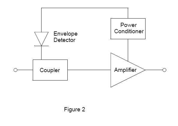
One exception is the idea of envelope elimination and restoration, which is being approached in a number of variants. In this idea, the signal is compressed, leaving only the phase information, and the amplitude information is restored by a more or less conventional amplitude modulation process (see Figure 2).
Although this approach seems simple and elegant, it suffers from a number of limitations, especially the need for a high efficiency, broadband modulator and the problem of phase shift introduced by the AM modulation process. Much of this can be addressed through DSP techniques. Other methods involve similar, direct phase- and amplitude-modulation of the PA. Again, DSP is necessary to overcome some of the difficulties.
Low Noise Amplifiers (LNA)
We have come a long way from the days when a low noise FET cost $300 and provided a 3 dB noise figure at 12 GHz, and we felt lucky to have it. Low noise GaAs, and even InP, FET technologies are mature, epitaxial MESFET technologies have almost completely given way to heterojunction technologies, and such devices are now available in low cost epoxy packages for a few cents each. Device noise figures, in the middle microwave region, are so low that the devices can be viewed as virtually noiseless, in that their noise is negligible relative to other noise sources. Similarly, the large-signal handling of such devices is indeed impressive, although it does come at the cost of DC power. As long as DC power is available, it is relatively easy to realize FET amplifiers with output third-order intercept points (IP3) above 40 dBm, although this generally occurs at some cost to the noise figure. Microwave FET amplifiers still must be optimized for high IP3 or low noise, but cannot be optimized for both. However, low device noise figure means that there is more room to trade off noise figure when the amplifier is optimized for IP3, showing that low noise provides a modest, albeit indirect, distortion benefit. But technical problems, like cockroaches, never disappear; they just find another place to reside. In this case, they have taken up residence in silicon, and now inhabit the land of CMOS and SiGe technology. Device noise figures inevitably fall as technology improves. Now, 0.15 μm CMOS technologies are considered standard tools, and much shorter gate technologies, 0.090 mm and even 0.065 mm, are available. The latter can produce circuits operating well into the millimeter region; indeed, 60 GHz circuits are readily produced in 0.13 mm technology.4 These technologies are valuable not only for low noise operation at high frequencies; they also provide high performance at low DC operating power. This is especially important for a wide variety of portable equipment. While reduction in noise figure is automatic as technologies improve, the same is not true of large-signal handling ability. Indeed, if anything, the use of smaller devices and lower operating voltages, necessary for these technologies, results in substantial reduction in large-signal capability. This comes from two characteristics. First, it is possible to show that scaling a particular device to a smaller size inherently decreases its linearity.5 If this scaling includes reduction in gate length as well as width, the nonlinearity becomes even more pronounced. Second, an amplifier’s output power is fundamentally limited by DC input power. As the signal level reaches a point where the amplifier cannot provide more output power, it saturates and the signal is distorted. Thus, even an ideally linear but power-limited amplifier must inevitably generate distortion as its output power approaches its limits. This has profound implications for LNAs in mobile, low power transceivers. Amplifiers in cell phones and computers, for example, must operate at very low DC power, but at the same time, must tolerate strong interfering signals. The communication techniques used in such applications are designed to be tolerant of interference from other users, but they cannot compensate for a signal completely blocking the front-end of the receiver. Thus, large-signal handling is an important requirement for such amplifiers, and, along with all the requirement of low DC power, a difficult one to meet. The DC power limitation is fundamental, so any way around it must involve increasing power, at least temporarily, in some manner. It is interesting to note that the research community seems to be addressing the matter of noise figure through technology improvements, but is not addressing the issue of large-signal handling and linearity in any non-obvious way. It seems, therefore, that some improvements might be possible if more fundamental research were applied to this problem.
Oscillator Technology, Design and Optimization
Oscillators are a mature technology. They have been around for a long time. It would therefore seem that, by now, we should have been able to figure out how they work. But we still have not. Lest the reader dismiss that remark as a provocative overstatement (which it is, after all, but please don’t dismiss it quite yet), consider this question: in how many areas of technology do we depend, for design information, on technical concepts that have not changed much in the last 40 years? Kurokawa theory,7 Barkhausen criterion,5 describing-function concepts8 and Leeson’s model of phase noise9 are still the dominant tools for oscillator design. Although it is true that new methods for oscillator and phase noise analysis have been developed,10–12 these are largely numerical means for computer-aided analysis of such circuits, and, with few exceptions (for instance in Refs. 13 to 17), provide little new, intuitive understanding of these components. Little new information has worked its way into the psyches of designers as general methods for designing and optimizing oscillators. The dominant approach for low noise oscillator design is to create negative resistance, maximize the Q of the tuning circuitry, minimize the noise through device selection, analyze it on the computer (as long as the device model includes low frequency noise sources; most do not) and hope for the best. If some designs work any better than others, it is not because of this kind of design process. One big hang-up is the idea of different types of designs. Four basic design approaches can be described: negative-resistance design, stemming from the ideas first proposed by Kurokawa;7 the use of Barkhausen’s criterion, which is a fundamental idea described in many texts;8 the use of classical circuit structures such as the Pierce and Colpitts structures; and, finally, the numerical formulations used in circuit simulators, harmonic-balance methods in particular. These have always been viewed as distinctly different design approaches, but, in fact, it is possible to show that they are equivalent. The Colpitts oscillator, for example, can be described as a feedback oscillator with an LC, pi-section feedback circuit.8,19 Rhea generalized this idea, showing that oscillators could use a wide variety of feedback circuits, many of which were more appropriate for certain applications or frequency ranges than the classic ones.20 These were inherently linear designs, but oscillators are strongly nonlinear circuits. These approaches depend on a concept called describing functions, in which the oscillator is modeled in terms of the circuit’s effect on the fundamental frequency alone. Although this approach provides some insight into their operation, oscillators, in reality, are nonlinear components and must be treated as such. Describing an oscillator’s operation in terms of changes in the fundamental-frequency component and behavior of pseudo-linear poles, as the active part of the circuit goes into oscillation, is a pretty severe oversimplification. Going beyond that kind of description requires consideration of the circuit’s nonlinearities.
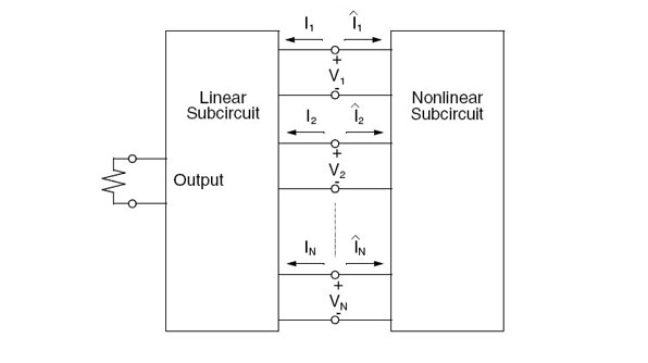
The equivalence of Rhea’s generalized feedback circuit (which, recall, is equivalent to the Barkhausen criterion), Kurokawa’s negative-resistance approach, and, finally, the modern harmonic-balance approach, are a little more difficult to see. Consider the classical division of a circuit into linear and nonlinear subcircuits for harmonic-balance analysis, as shown in Figure 3.
It applies to oscillators as well as driven circuits. In the oscillator case, there are no excitations. (We assume that the DC excitation is inherent in the negative-resistance device and need not to be shown explicitly.) This division is basic to harmonic-balance analysis. Let Z be the impedance matrix of the linear subcircuit and Y be the admittance matrix of the linearized nonlinear subcircuit. Clearly,
V = ZI (1)
For oscillation to occur, the voltages at the nonlinear subcircuit must produce the set of harmonic current components that satisfy Equation 1. This is equivalent to saying that the voltage produces a current, from the active element, which in turn produces that same voltage after feedback, a statement, in effect, of the Barkhausen criterion. This is the basis of the feedback description. Thus,
–I = YV (2)
From Equations 1 and 2,
–ZYV = V (3)
Thus, oscillation conditions for the linear oscillator require that the matrix –ZY have an eigenvalue equal to 1. Reducing this to Kurokawa’s negative-resistance case of a single port and a single frequency (the fundamental, of course), we have
–ZL Ys V = V (4)
or
ZL = –Zs (5)
which is the well known oscillation condition for negative-resistance oscillators.
This simple derivation also shows why a purely linear oscillator cannot exist: the voltage vectors satisfying Equation 3 are eigenvectors of the system, which are never unique. Thus, a unique oscillatory solution does not exist. Some nonlinearity is necessary to create a unique solution. In the nonlinear case, Equation 3 becomes
–Z FI(V) = V (6)
where FI(V) is a nonlinear vector function, providing harmonic element currents as a function of harmonic voltages. Although I start to bleed internally while doing this, it is possible to express Equation 6 in this form
–Z Y(V) V = V (7)
generalizing the describing-function approach, which is based on the idea of a fundamental-frequency, psuedo-linear circuit whose admittances depend on voltage magnitude.
Nonlinear analysis of oscillators

My favorite way to illustrate the problems of nonlinear oscillator analysis is through an example, the Van der Pol oscillator. The Van der Pol oscillator is beloved of circuit theorists because it can be treated analytically, without resorting to numerical methods. The oscillator is shown in Figure 4. It consists of a nonlinear, negative-resistance device having the I/V characteristic
I(V) = –GV + GaV3 (8)
and an ordinary parallel LC resonator. We assume that this resonator is high Q, so only a single harmonic of voltage can exist; thus,
V(t) = V1 cos(wt) (9)
Substituting this into Equation 8 shows that only first- and third-harmonic currents exist, and the latter simply idle in the resonator. Satisfying Kirchoff’s current law and solving for V1 gives the simple result
V1 = [4/3 (G – GL)/Ga]1/2 (10)
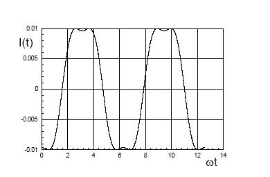
Applying some numbers to Equation 10, G = 0.015, GL = 0.01 and a = 1/3, gives V1 = 1.1547 V. The device-current waveform is shown in Figure 5 and its fundamental-frequency component is I1 = –0.01547 A. Note that we have satisfied the oscillation conditions in the negative-resistance sense, as the device admittance (defined as in Kurokawa’s theory) is I1/V1 = –0.01 = –GL. Note also that the device’s small-signal admittance, found by differentiating Equation 8, is –0.015. Thus, the magnitude of the small-signal conductance has decreased, as the voltage magnitude increased, as required by negative-resistance oscillator theory. The figure gives a good, intuitive sense of why this occurs: as V1 increases, the current waveform flattens, and its fundamental-frequency component no longer increases as rapidly as V1. Therefore, |I1/V1| inevitably decreases, until an equilibrium is reached that satisfies the oscillation conditions. This idea contradicts a commonly held belief about transistor oscillators, namely, that the circuit, unstable in the small-signal sense, “blows up,” and is saved from oblivion only by saturation of the active device. In reality, a kind of nonlinear balancing act occurs, with the venerable Kirchoff doing the balancing. The whole process is really quite civilized, and thoroughly non-violent.
The circuit has other stories to tell, which are profoundly important for oscillator analysis. To do so, we put the circuit into harmonic-balance form, create the Jacobian, and discover that, when the oscillation conditions are satisfied, the Jacobian is singular! In practice, this means that oscillator analysis, by harmonic-balance methods, is inherently numerically ill conditioned, and its ill conditioning gets worse as the iterative process approaches a solution. This is one reason why nonlinear analysis of oscillators is so difficult. However, one can also show that when the nonlinear analysis problem is formulated as an optimization problem, instead of the more traditional multi-dimensional Newton approach, the problem is much better conditioned. This may be one reason why methods based heavily on optimization, such as the use of an auxiliary generator, seem to be considerably more robust than those based more strongly on Newton’s method.
Phase Noise Analysis
One of the more contentious research subjects has been the matter of phase noise analysis and optimization. As such, it is interesting to view this situation both historically and technically.
One of the earliest treatments of phase noise in oscillators, and often the only one familiar to designers, is that of Leeson.9 Leeson formulated the oscillator noise problem as a kind of phase feedback circuit containing an amplifier and resonator, in which noise was treated as an input signal near the frequency of oscillation.
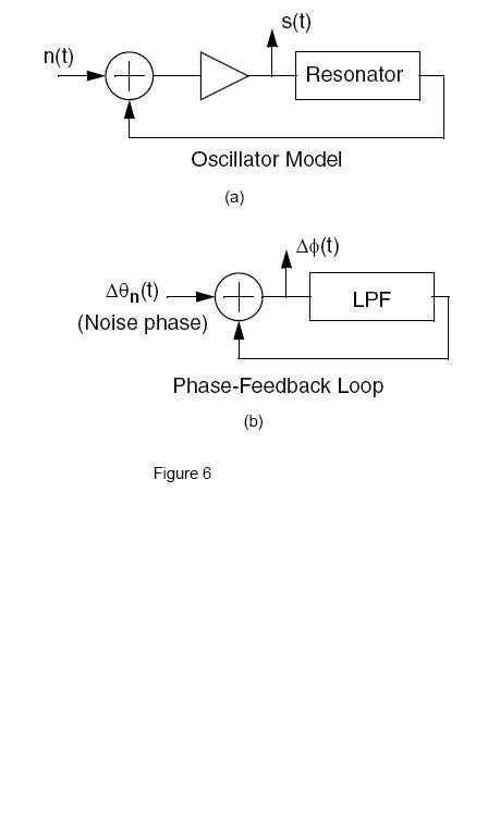
The model is shown in Figure 6. Analyzing this model by a baseband equivalent circuit, and assuming the noise spectrum to have a 1/f shape, gives Leeson’s well known expression for the SSB carrier-to-noise ratio, £(fm),

where Ps is the signal power, QL is the loaded Q of the resonator, fm is the offset frequency and f0 is the frequency of oscillation. F is called the noise figure, but it is actually a measure of the level of upconverted 1/f noise; it is decidedly not the high frequency noise figure of the amplifier.
This model essentially tells us that, for a particular frequency of oscillation and offset frequency, we should maximize the signal-to-noise ratio and minimize the loaded Q of the resonator, both of which seem intuitively reasonable. The model, however, is not quantitatively very useful, as it does not tell us anything about the upconversion process of 1/f noise from baseband to the oscillation frequency, and the concept of “loaded Q,” while clear in the model, is not clear in a real oscillator circuit; the loaded Q of a negative-resistance oscillator is always infinite! Thus, while useful qualitatively, Leeson’s model has no real quantitative value.
A more complete phase noise analysis has been a research goal for many years. One of the most interesting early works was that of Rizzoli, et al.,21 who discovered that ordinary, nonlinear-noise theory, applied to oscillators, simply did not work at low offset frequencies. They did discover, however, that an alternative but equivalent method, based on phase sensitivities, worked well at those small offsets. Thus arose the dichotomy between conversion noise, the standard method and modulation noise, based on phase sensitivities. Many of today’s harmonic-balance phase noise analyses still use these concepts. The problem with conversion noise at small offsets is closely related to the problem of Jacobian singularity. The conversion matrix, used in the conversion-noise analysis, is, in effect, a Jacobian evaluated at the offset frequency.

Thus, the smaller the offset, the worse the Jacobian conditioning, and the less stable the solution. This can be illustrated dramatically with the Van der Pol oscillator. Figure 7 shows the results of a conversion-noise analysis of the oscillator (a), which seems quite credible. However, changing a single term of the conversion matrix from 0.005 to 0.005000001 gives the result shown in (b). The original calculation seems right only because the analysis of the Van der Pol oscillator can be performed analytically, and, fortuitously, the matrix entries can be expressed exactly with few decimal places. Note, however, that the graphs are identical beyond 10 kHz. This is typical of conversion-noise analysis. The dual treatment of conversion and modulation noise has always presented a small, but real, dilemma: at what point does one switch from one type of analysis to another? It is not always clear that the intuitive answer to that question is really the correct one. It is better to have one analysis that unifies the two. One such method, which has been implemented in more modern circuit simulators, is that of Ngoya.22 Experience indicates that this method is quite robust and accurate at all offset frequencies.
Oscillator Design and Optimization
These methods, while important for numerical analysis of oscillators, provide little insight into design techniques for minimizing phase noise. Surprisingly, only a little work based on ideas other than manipulation of Leeson’s model has been presented. One exception is the work of Zirath, et al., who showed that millimeter-wave oscillator phase noise, in both SiGe and InGaP HBT technologies, could be minimized through the use of a small set of thoroughly straightforward design methods. One of their VCOs exhibited –120 dBc noise at 100 kHz offset, at an output frequency of 13 GHz.17,18 One of the clear implications of Leeson’s model, as well as other approaches to phase noise analysis, is the need for a high resonator Q. High resonator Q not only minimizes phase noise, but makes the oscillator’s stability (which is, in reality, a kind of phase noise at low offset frequencies) more a function of the resonator’s characteristics and less of the device’s. The latter, of course, is thermally relatively unstable, so it is beneficial to make the oscillator’s performance dependent primarily on a stable, well designed resonator.
Unfortunately, making a good resonator is not easy, especially if small size and complete integration is needed. Most high performance oscillators today use dielectric resonators coupled to microstrip. These must be shielded and located off-chip, so even a monolithic oscillator incurs the cost of a special housing and extra components. Worse, optimizing the dielectric resonator’s coupling to the microstrip line usually requires a degree of manual adjustment, the last thing one desires in low cost, high volume production. Thus, the research literature is heavy with attempts to create high quality (or, shall we say, acceptable-quality) resonators on-chip. This need is especially great in silicon RF CMOS and BiCMOS, where virtually every chip needs the high stability, frequency accuracy and low phase noise provided by a phase-locked loop. Inevitably, the on-chip resonator is an LC circuit using a spiral inductor. Because of the inherently lossy substrates and conductors used in CMOS circuits, such inductors do not have high Qs. Much research has been devoted to optimizing those inductors.23–27 Some of this work has been quite sophisticated analytically,28 and a wide variety of circuits have been produced.29–33 Other work has been devoted to finding other ways to make tunable reactive elements34 or integrating more conventional resonators into fabrication media, obviating the need for resonator tuning.35
Oscillators and Amplifiers at Millimeter Wavelengths
One of the most remarkable developments of the past few years has been the ability to fabricate millimeter-wave (mmW) circuits in silicon CMOS. The sophistication of silicon technology, allowing thin oxides and feature sizes well below 0.1 mm, with good yield, allows practical circuits well above 100 GHz. Although many difficulties remain, such capabilities indicate that commercial mmW applications may exist in the near future. At the same time, modern circuit-analysis and electromagnetic-analysis software is instrumental in addressing the very difficult problems of low cost, practical circuit interfaces and packaging. Automotive applications serve as a prototype for the commercial exploitation of such technologies. The obvious one is the automotive radar band at 77 GHz. GaAs and InP heterojunction technologies have been, and probably always will be, too expensive for making automotive radars that can be installed in all types of vehicles. Silicon will probably be necessary for a broad application of such systems. Similarly, many types of automotive sensors, such as anti-theft devices and backup and blind-spot warning sensors, already exist, albeit only in high end vehicles. Cost reductions likely from silicon mmW realizations may make these more generally available, improving security and safety of many kinds of vehicles. Another important application is millimeter-wave imaging for security purposes. Such systems already exist, but they are often too expensive for small-scale use. One of the most important advantages of mmW technology is the availability of broad bandwidths. This is especially important for one of the more interesting applications, point-to-point and point-to-multipoint high data-rate communications at 60 GHz. The 60 GHz band offers up to 7 GHz of spectrum for such applications. Paradoxically, the high loss caused by oxygen absorption at this frequency often is an advantage. It creates an exponential loss component on top of the ordinary inverse-square loss due to range, which can be used, along with power adjustment, to minimize interference. Such techniques have been of interest to the military, for secure communications, for many years. A recent workshop at the 2006 European Solid-state Circuits Conference in Montreux, Switzerland, showed that, although packaging and interfacing issues remain, silicon IC technologies are largely mature enough for the development of commercial circuits. Papers at the conference described, for example, 20 and 77 GHz automotive sensors37,38 and a 60 GHz power amplifier39 with surprisingly good performance. Other conferences and journals have offered similarly encouraging results, including work on the packaging problem.4,40–50 It appears that millimeter waves may no longer be the perpetual technology of the future.
Conclusion
Amplifiers and oscillators, while seemingly mature technologies, are still subjects of great importance and substantial research. Efficiency and linearity in power amplifiers, performance of high frequency LNAs in silicon CMOS, and all aspects of low noise oscillator design and analysis are areas of great interest, both in terms of practical needs and research interest. We should see some exciting results in these areas in the next few years.
References
- P. Zampardi, “Performance and Modeling of Si and SiGe for Power Amplifiers,” SiRF2007 Conference Digest.
- S. Cripps, “RF Power 2005,” Microwave Journal, Vol. 48, No. 4, April 2005, pp. 22–36.
- S. Cripps, RF Power Amplifiers for Wireless Communications, Second Edition, Artech House, Norwood, MA, 2006.
- B. Floyd, et al., “Silicon Millimeter-wave Radio Circuits at 60 to 100 GHz,” SiRF2007 Conference Digest.
- S.A. Maas, Nonlinear Microwave and RF Circuits, Artech House, Norwood, MA, 2003.
- 6. M. El Kaamouchi, et al., “A 2-mW Power Consumption Low Noise Amplifier in PD SOI CMOS Technology for 2.4 GHz Applications,” SiRF2007 Conference Digest.
- 7. K. Kurokawa, “Some Basic Characteristics of Broadband Oscillator Circuits,” Bell System Technical Journal, Vol. 48, pp. 1937–1969.
- 8. G. Gonzalez, Foundations of Oscillator Circuit Design, Artech House, Norwood, MA, 2007.
- 9. D.B. Leeson, “A Simple Model of Feedback Oscillator Noise Spectrum,” Proceedings of the IEEE, Vol. 54, 1966, p. 329.
- 10. E. Ngoya, et al., “Steady State Analysis of Free or Forced Oscillators by Harmonic Balance and Stability Investigation of Periodic and Quasiperiodic Regimes,” International Journal of Microwave and Millimeter-wave Computer Engineering, Vol. 5, 1995, p. 210.
- 11. V. Rizzoli, et al., “Optimization-oriented Design of Free-running and Tunable Microwave Oscillators by Fully Nonlinear CAD Techniques,” International Journal of Microwave and Millimeter-wave Computer Engineering, Vol. 7, 1997, p. 52.
- 12. C.R. Chang, M.B. Steer and E. Reese, “Computer-aided Analysis of Free-running Microwave Oscillators,” IEEE Transactions on Microwave Theory and Techniques, Vol. 39, No. 10, October 1991, pp. 1735–1745.
- 13. A. Hajimiri and T.H. Lee, The Design of Low Noise Oscillators, Kluwer, Boston, 1999.
- 14. J.K.A. Everard, “Low Noise Oscillators,” 1992 IEEE MTT-S International Microwave Symposium Digest, Vol. II, pp. 1077–1080.
- 15. S. Alechno, “Oscillators: A New Look at an Old Model,” Microwaves and RF, December 2002, p. 51.
- 16. A.V. Grebennikow, “Microwave Transistor Oscillators: An Analytic Approach to Simplify Computer-aided Design,” Microwave Journal, Vol. 42, No. 5, May 1999,
pp. 292–300. - 17. H. Zirath, R. Kozhuharov and M. Ferndahl, “Balanced Collpitt Oscillator MMICs Designed for Ultra-low Phase Noise,” IEEE Journal of Solid-state Circuits, Vol. 40, 2005, p. 2077.
- 18. H. Zirath, et al., “MMIC Oscillator Designs for Ultra-low Phase Noise,” 2005 IEEE Compound Semiconductor Integrated Circuit Symposium Digest, p. 204.
- 19. M. Ghausi, Electronic Circuits, Van Nostrand, New York, NY, 1971.
- 20. R. Rhea, Oscillator Design and Computer Simulation, Second Edition, McGraw-Hill, New York, NY, 1995.
- 21. V. Rizzoli, et al., “Harmonic-balance Optimization of Microwave Oscillators for Electrical Performance, Steady-state Stability and Near-carrier Phase Noise,” 1994 IEEE MTT-S International Microwave Symposium Digest, Vol. III, pp. 1401–1404.
- 22. E. Ngoya, J. Rousset and D. Argollo, “Rigorous RF and Microwave Oscillator Phase Noise Calculation by Envelope Transient Techniques,” 2000 IEEE MTT-S International Microwave Symposium Digest, Vol. I, pp. 91–94.
- 23. A. Telli, I.E. Demir and M. Askar, “Practical Performance of Planar Spiral Inductors,” Proceedings of the 11th IEEE International Conference on Electronics, Circuits and Systems, 2004, p. 48.
- 24. B.L. Ooi, D.X. Xu and P.S. Koo, “A Comprehensive Explanation on the High Quality Characteristics of Symmetrical Octagonal Spiral Inductor Radio Frequency Integrated Circuits,” 2003 RFIC Symposium Digest, p. 259.
- 25. Z. Zhang, et al., “Optimization of Q Factor in Spiral Inductors on Silicon,” Proceedings of the 6th International Conference on Solid-state and Integrated-circuit Technology, 2001, p. 251.
- 26. K. Murata, T. Hosaka and Y. Sugimoto, “Effect of a Ground Shield of a Silicon On-chip Spiral Inductor,” 2000 Asia-Pacific Microwave Conference Digest, p. 177.
- 27. A. Nieuwoudt and Y. Massoud, “Multi-level Approach for Integrated Spiral Inductor Optimization,” Proceedings of the Design Automation Conference, 2005, p. 648.
- 28. C.R. deRanter, et al., “CYCLONE: Automated Design and Layout of RF LC-Oscillators,” IEEE Transactions on Computer-aided Design of Integrated Circuits and Systems, Vol. 21, 2002, p. 1161.
- 29. I.R. Chamas and S. Raman, “A 5 GHz I/Q Phase-tunable CMOS LC Quadrature VCO (PTQVCO) for Analog Phase Calibrated Receiver Architectures,” SiRF2007 Conference Digest.
- 30. Satoshi Kurachi, et al., “5 GHz Band Highly Linear VCO IC with a Novel Resonant Circuit,” SiRF2007 Conference Digest.
- 31. B. Soltanian and P. Kinget, “A Low Phase Noise Quadrature LC VCO Using Capacitive Common-source Coupling,” 2006 European Solid-state Circuit Conference Digest, p. 436.
- 32. C. Cao, E. Seok and K.K. O, “Millimeter-wave CMOS Voltage-controlled Oscillators,” 2007 IEEE Radio and Wireless Symposium Digest, p. 185.
- 33. A. Maxim, “A 10 GHz, 0.11 mm CMOS Varactorless LC VCO for Multi-standard 802.11a/b/g WLAN Using High Resolution Frequency Calibration,” 2007 IEEE Radio and Wireless Symposium Digest, p. 189.
- 34. J. Laskar, R. Mukhopadhyay and C.H. Lee, “Active Inductor-based Oscillator: A Promising Candidate for Low Cost, Low Power, Multi-standard Signal Generation,” 2006 European Solid-state Circuits Conference Digest, p. 31.
- 35. S.A. Maas, J. Delacueva, J. Li and S. White, “A Low Cost, Cavity-stabilized 5.8 GHz Oscillator Realized in LTCC,” Microwave Journal, Vol. 44, No. 4, April 2001, pp. 130–134.
- 36. L.M. Franca-Neto and D. Belot, “1Gbit/s+ Wireless Communications at 60 GHz and Beyond,” 2006 European Solid-state Circuits Conference.
- 37. M. Berry, et al., “Integrated RF Front-end in 0.13 mm CMOS for Automotive and Industrial Applications Beyond 20 GHz,” 2006 European Solid-state Circuits Conference Digest, p. 392.
- 38. L. Wang, J. Borngraeber and W. Winkler, “77 GHz Automotive Radar Receiver Front-end in SiGe:C BiCMOS Technology,” 2006 European Solid-state Circuits Conference Digest, p. 388.
- 39. U. Pfeiffer, “A 20 dBm Fully-integrated 60 GHz SiGe Power Amplifier with Automatic Level Control,” 2006 European Solid-state Circuits Conference Digest, p. 356.
- 40. U. Pfeiffer, et al., “A Chip-scale Packaging Technology for 60 GHz Wireless Chipsets,” IEEE Transactions on Microwave Theory and Techniques, Vol. 54, No. 12, December 2006, p. 3387.
- 41. C.C.E. Seok and K.K. O, “Millimeter-wave CMOS Voltage-controlled Oscillators,” 2007 Radio and Wireless Symposium Digest, p. 185.
- 42. S.E. Gunnarsson, et al., “Highly Integrated 60 GHz Transmitter and Receiver MMICs in a GaAs pHEMT Technology,” IEEE Journal of Solid-state Circuits, Vol. 40, 2005, p. 2174.
- 43. A. Maxim, et al., “Fully Integrated 0.13 mm CMOS Digital Low-IF DVB-S/S2 Satellite TV Tuner Using a Discrete-Step AGC Loop,” 2007 IEEE Radio and Wireless Symposium Digest, p. 67.
- 44. S.S. Taylor and A. Waltho, “Multi-radio Platforms in Scaled CMOS Technology,” SiRF2007 Conference Digest.
- 45. M. Gu, et al., “A Wideband Front-end for Terrestrial and Cable Receptions,” SiRF2007 Conference Digest.
- 46. B. Floyd, et al., “A Silicon 60 GHz Receiver and Transmitter Chipset for Broadband Communications,” 2006 IEEE International Solid-state Circuits Conference Digest, p. 184.
- 47. J. Grzyb, D. Liu, U. Pfeiffer and B. Gaucher, “Wideband Cavity-backed Folded Dipole Superstrate Antenna for 60 GHz Applications,” Proceedings of the Applied Physics Society, July 2006.
- 48. W. Winkler, J. Borngräber, H. Gustat and F. Korndörfer, “60 GHz Transceiver Circuits in SiGe BiCMOS Technology,” 2004 European Solid-state Circuit Conference Digest, p. 83.
- 49. Y.M. Sun, J. Borngräber, F. Herzel and W. Winkler, “A Fully Integrated 60 GHz LNA in SiGe:C BiCMOS Technology,” 2005 IEEE Bipolar/BiCMOS Circuits and Technology Meeting, p. 14.
- 50. L. Wang, R. Kraemer and J. Borngraeber, “An Improved Highly-linear Low Power Down-conversion Micromixer for 77 GHz Automotive Radar in SiGe Technology,” 2006 IEEE MTT-S International Microwave Symposium Digest.

Stephen Maas received his BSEE and MSEE degrees in electrical engineering from the University of Pennsylvania in 1971 and 1972, respectively, and his PhD degree in electrical engineering from UCLA in 1984. Since then, he has been involved in the research, design and development of low noise and nonlinear microwave circuits and systems at the National Radio Astronomy Observatory (where he designed the receivers for the Very Large Array), Hughes Aircraft Co., TRW, the Aerospace Corp. and the department of electrical engineering at UCLA. Subsequently he worked as an engineering consultant and founded Nonlinear Technologies Inc., a consulting company, in 1993. He recently became chief scientist of Applied Wave Research Inc. He is the author of Microwave Mixers (Artech House, 1986 and 1992), Nonlinear Microwave Circuits (Artech House, 1988; second edition 2003), The RF and Microwave Circuit Design Cookbook (Artech House, 1998) and Noise in Linear and Nonlinear Circuits (Artech House, 2005). From 1990 until 1992 he was editor of the IEEE Transactions on Microwave Theory and Techniques and from 1990 to 1993 was an Adcom member and Publications Chairman of the IEEE MTT Society. He received the Microwave Prize in 1989 for his work on distortion in diode mixers and the MTT Application Award in 2002. He is a Fellow of the IEEE.