
A single-feed patch antenna with circular polarization (CP) and slot loading is introduced, featuring an I-shaped slot etched on the radiating patch, which introduces mutually orthogonal modes. A crossed slot on the ground plane, coupled with an annular ring microstrip feed line, forms the feed structure. This mechanism simultaneously excites two orthogonal modes with a 90-degree phase difference, resulting in CP radiation. Measurements demonstrate a 25.56 percent 3 dB axial ratio bandwidth and a 32.5 percent 10 dB impedance bandwidth. Gain reaches 9.2 dBi at 3.58 GHz. The antenna’s size is 0.84 × 0.65 × 0.067 λo3 with λo defined as the wavelength at 3.48 GHz.
Due to its compact size and simple structure, the patch antenna is commonly used in various wireless communication systems, such as satellite and aviation communications.1-3 Conventional design methods for CP patch antennas typically achieve an operational bandwidth of only around 0.7 percent, which limits their use in practical applications.4
To broaden the operational bandwidth, parasitic components or etched slots are incorporated into the antenna structure.5-9 Wu et al.5 proposed a CP patch antenna using a capacitively coupled feed and four parasitic strips, resulting in an enhanced axial ratio bandwidth (ARBW). Ding et al.6 employed parasitic elements and a feed ring placed on the same plane, achieving a broad ARBW. Lin and Chu7 significantly improved antenna ARBW from 1.3 to 3.3 percent by incorporating parasitic structures. Hao et al.8 generated CP in a single-feed antenna through an etched slot on the patch, yielding a 5.4 percent ARBW. Wang et al.9 used a ground plane with four slots, which further extended the ARBW compared to a fully grounded plane.6
CP can be achieved with power dividers.10,11 Chen et al.10 used a power divider to extend the ARBW of a patch antenna, yielding an impedance bandwidth of approximately 10.6 percent (from 870 to 967 MHz) and an ARBW of about 6 percent (from 893 to 948 MHz). Despite the improved bandwidth, however, the antenna was relatively large (220 × 220 × 14 mm3). Kim and Kim11 used a ring structure to achieve a 90-degree phase shift and employed a Gysel power divider, resulting in 71.7 percent impedance bandwidth and 29.7 percent ARBW. A metal reflector was placed underneath the antenna to enhance its overall gain; however, using a thicker substrate introduced additional difficulties in the manufacturing process.
Multilayer designs have been widely used to improve the performance of single-fed CP patch antennas.12-20 Deng et al.14 used a corner-truncated ring to simplify the feed structure. It achieved a 20.6 percent impedance bandwidth and an ARBW of approximately 6.94 percent by incorporating corner truncations and L-shaped branches on the radiating patch. Liu et al.16 introduced a high gain CP patch antenna by adopting a stacked patch structure with pin loading. Li et al.17 demonstrated significant performance improvements by incorporating an L-shaped stub. The antenna achieved an impedance bandwidth of approximately 42.1 percent and an ARBW of about 26.0 percent with a maximum gain of 8.6 dBiC.
Multiple feed techniques are effective in extending ARBW.21,22 Lin et al.21 proposed a wideband tri-fed CP antenna achieving a 47.88 percent ARBW with three symmetric feed points 120 degrees apart. Tamjid et al.22 described a quad-fed CP antenna achieving 32.5 percent impedance bandwidth and a peak gain of 7.33 dBic using two coupled-line power dividers. However, the feeding network design was complex.
A single-feed CP patch antenna with a compact structure and wide bandwidth is proposed in this work. The design incorporates a slotted radiating patch, an annular ring microstrip feed line and a ground plane with a crossed slot, resulting in a simplified structure. The annular ring microstrip feed line is aperture-coupled to the radiating patch through a cross-shaped slot, which enables CP radiation. Measurements yield a 32.5 percent impedance bandwidth (from 3.45 to 4.79 GHz) with |S11| below -10 dB, and a 25.56 percent ARBW (from 3.48 GHz to 4.5 GHz), with the AR below 3 dB.
ANTENNA DESIGN
Figure 1a shows a side view of the antenna, consisting of Layer_1, an air gap, Layer_2 and Layer_3, with the height of the air gap between Layer_1 and Layer_2 denoted as h1. The bottom of Layer_2 features a ground plane with a crossed slot (see Figure 1b). Figure 1c shows the annular microstrip feed line at the bottom of Layer_3. Figure 1d shows the rectangular patch on Layer_1, which is etched with an I-shaped slot.
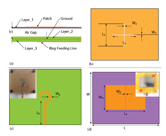
Figure 1 Antenna structure: (a) side view, (b) lower view of the second layer, (c) lower view of the third layer and (d) upper view of the first layer.
The annular ring microstrip feed line is aperture-coupled to the patch through the crossed slot, enabling the generation of CP radiation. The εr value of Layer_1 is 2.32, with a thickness of 0.5 mm. Layer_2 and Layer_3 have εr values of 3.55, each with a thickness of 1 mm. The optimized geometrical parameters are (in mm): W4 = 26, L4 = 42, W5 = 0.4, W = 56, L = 72, W3 = 0.9, L3 = 24, W2 = 0.5, L2 = 26, h1 = 3.2, W6 = 2.2 and L5 = 24.2.
Figure 2 shows the surface current distributions of the two orthogonal modes (Modes 1 and 2) introduced by the I-shaped slot. The red arrows indicate the directions of the surface currents associated with these modes. Mode 1 corresponds to the TM01 mode, while Mode 2 is a new mode introduced by the I-shaped slot.
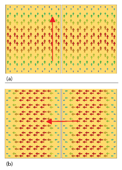
Figure 2 Modal surface current distribution: (a) Mode 1 and (b) Mode 2.
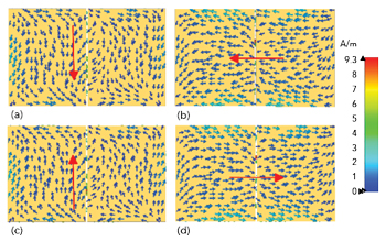
Figure 3 Patch surface current distribution as a function of time: (a) t=0, (b) t=T/4, (c) t=T/2 and (d) t=3T/4. (T = period at 4 GHz).
Generating CP requires exciting two orthogonal modes with equal amplitudes and a 90-degree phase difference. According to the magnetic field coupling excitation method, excitation is applied to regions with stronger currents.23 Therefore, a cross-shaped slot is etched on the ground plane, and both modes are simultaneously excited using an annular microstrip feed line. By appropriately adjusting the length of the cross-shaped slot, the phase difference of radiation in the far-field can be tuned to approximately 90 degrees.
To better understand the CP radiation mechanism, simulation over time is performed at 4 GHz (see Figure 3). In Figures 3a and 3b, the current directions are orthogonal to each other. In Figures 3c and 3d, the current magnitudes remain unchanged, but their directions are reversed with respect to Figures 3a and 3b. This clockwise rotation of the surface current over time results in left-handed circular polarization (LHCP) radiation.
PARAMETRIC STUDIES
When L2 is increased from 25 mm to 27 mm, |S11| decreases at higher frequencies and increases at lower frequencies, with the resonant frequency shifting to lower values. This is due to the slot altering the current distribution and effective electrical length of the antenna. As L2 increases, the AR minimum points also shift to lower frequencies, with optimal performance at L2 = 26 mm (see Figure 4a).
As W2 increases from 0.4 mm to 0.6 mm, |S11| in the high frequency band increases, where |S11| in the low frequency band shows almost no change (see Figure 4b). Additionally, the AR is almost unaffected as W2 increases. To optimize the impedance bandwidth, the width of the slot is determined to be 0.5 mm.
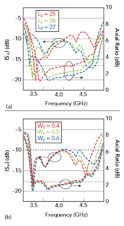
Figure 4 Effect of (a) slot length (L2) and (b) slot width (W2) on |S11| and AR.
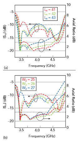
Figure 5 Effect of (a) patch length (L4), and (b) patch width (W4) on |S11| and AR.
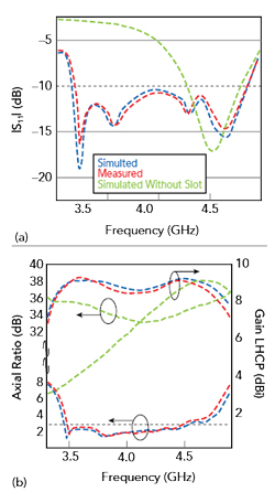
Figure 6 Simulated and measured results: (a) |S11| and (b) AR and gain.
Increasing L4 from 41 mm to 43 mm reduces |S11| at low frequencies but has little effect at high frequencies, with the 3 dB ARBW narrowing (see Figure 5a). The optimal performance is achieved at L4 = 42 mm.
As W4 increases from 25 to 27 mm, |S11| is above -10 dB at 4.13 GHz for W4 = 25 mm and at 3.5 GHz for W4 = 27 mm. Optimal CP performance is for W4 = 26 mm (see Figure 5b).
The analysis of these four parameters indicates that the AR is primarily influenced by the slot length and the length of the radiating patch. When the lengths of the slot and patch are suitably adjusted, the phase difference between the two orthogonal modes is altered, which in turn affects the AR. By adjusting the lengths of the cross-shaped slot and the radiating patch, the phase difference in the far-field is effectively tuned to approach 90 degrees, thereby enhancing the generation of CP radiation.
EXPERIMENTAL RESULTS
The antenna resonates only at 4.51 GHz when the radiating patch is not etched with slots (see Figure 6). The introduction of an I-shaped slot at the center of the patch leads to the emergence of three additional resonant frequencies at 3.5, 3.75 and 4.32 GHz, resulting in broadband performance. Measured values of |S11|, AR and gain show close agreement. The measured -10 dB impedance bandwidth is approximately 32.5 percent (from 3.45 to 4.79 GHz). Similarly, the measured 3 dB ARBW is approximately 25.56 percent (from 3.48 GHz to 4.50 GHz). The antenna demonstrates excellent gain performance across the operating band, with a peak gain of approximately 9.2 dBi at 3.58 GHz.