

As higher data rate communication emerges, there will be extraordinary growth of 5G mmWave filters from $0.1 billion in 2024 to an expected $1.39 billion by 2033 with a CAGR of 35.8 percent.¹ This growth indicates the critical importance of these components in next-generation wireless infrastructure. With the progression toward 6G systems operating at frequencies above 100 GHz, the design and development of microwave filters encounter increasingly challenging requirements, necessitating the adoption of advanced and innovative engineering solutions.
The mmWave spectrum, particularly the 5G new radio (NR) frequency bands including n257 (28 GHz), n258 (26 GHz), n260 (39 GHz) and n261 (27 GHz), presents unique propagation characteristics and technical requirements. 6G technology focuses on faster and smarter communication. One of the frequency ranges is the D-Band (110 to 170 GHz), which supports the transfer of massive data quickly. Another range is the sub-terahertz range (100 to 300 GHz), which is useful for both high speed, short-distance communication and advanced sensing, such as gesture recognition or 3D imaging. It also faces signal loss, which has prompted researchers to work vigorously on integrated optical-wireless systems that combine the speed of optical fiber with the flexibility of wireless signals.
mmWave filters are important passive components in both 5G and 6G communication systems due to their precise signal selection and interference suppression at high frequencies. As communication progresses into the mmWave bands (above 24 GHz for 5G and beyond 100 GHz for 6G), filters are essential to isolate the frequency channels. This is important due to higher signal attenuation, dense spectrum usage and increased sensitivity to noise and interference. They also support multiband and wideband operation, which helps achieve high data rates and low latency assured by 5G and 6G systems. Without effective filtering, hardware constraints, out-of-band noise and signal overlap would cause the performance to deteriorate. As a result, filters are crucial to maintain the selectivity, speed and dependability of sophisticated wireless communication systems.
A comprehensive analysis of current mmWave filter technologies is provided in this article, with a focus on design strategies, performance tradeoffs and emerging trends that will impact the advancement of 5G and 6G communications.
Design Challenges
Developing filters at mmWave frequencies presents several challenges due to the exclusive behaviour of electromagnetic waves at high frequencies. Figure 1 depicts the critical design challenges of mmWave filters.
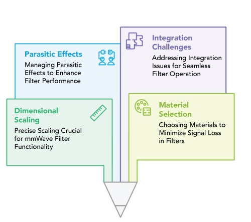
Figure 1 Design challenges of mmWave filters.
Scaling and Manufacturing Tolerances
At lower frequencies, manufacturing tolerances are generally negligible, whereas at mmWave frequencies, they become critical design parameters. For a 28 GHz filter, variations of ±10 μm in critical dimensions can shift the center frequency by several hundred MHz. This necessitates the utilization of advanced lithographic processes with sub-micron resolution, tight control of substrate thickness variations (±5 μm), precise via diameters and pitch control in multilayer structures.
Material Selection and Loss Mechanisms
Due to the greater influence of conductor and dielectric losses, identifying suitable substrate materials becomes crucial at mmWave frequencies.
To guarantee low signal attenuation and excellent filter performance, low loss substrates are essential. Commonly used materials include Rogers RT/Duroid 5880 with a dielectric constant (εr) of 2.2 and a loss tangent (tan δ) of 0.0009,2 liquid crystal polymer (LCP) with εr = 3.0 and tan δ = 0.002,3 fused silica glass (εr = 3.8, tan δ = 0.0001) and AlN ceramics (εr = 8.8, tan δ = 0.0001).
Due to the skin effect, the conductor loss plays a vital role in mmWave filters. At 28 GHz, the skin depth in copper reduces to approximately 0.35 μm, making the surface roughness of conductors a significant contributor to the overall loss. To mitigate this, advanced metallization techniques are employed, such as electroplated gold surfaces for ultra-low loss, chemical-mechanical polishing for surface planarization and the use of silver-based conductors to enhance conductivity.4,5 These measures collectively help in maintaining filter efficiency and performance at mmWave frequencies.
Parasitic Effects and Coupling
At mmWave frequencies, parasitic effects and undesirable coupling will reduce the filter’s performance. Package parasitic effects like bond wire inductance are non-negligible and should be carefully modelled, as they will provide undesirable reactance in the component. Another consideration is the via discontinuities in multilayer structures, as they introduce spurious resonances and unwanted coupling paths.4 This degrades the filter response. Radiation loss and insufficient shielding require robust electromagnetic isolation.
Integration Challenges
The progression towards high performance 5G/6G systems leads to new issues in integration. When filters and amplifiers are designed together, impedance matching and overall system stability must be considered.6 Integration of antennas and filters reduces the size and insertion loss but enhances the complexity.7 System-on-package (SoP) is a technique widely used to integrate numerous RF components, such as filters, mixers and amplifiers in a single module.8 However, this density requires well-organized thermal management methodologies to dissipate heat and to avoid a decline in functionality due to the temperature rise.9 To ensure the dependability and effectiveness of mmWave front-end modules, these issues must be addressed.
FILTER TECHNOLOGIES FOR 5G
There are various technologies used to develop 5G mmWave filters. The prominent technologies are depicted in Figure 2.
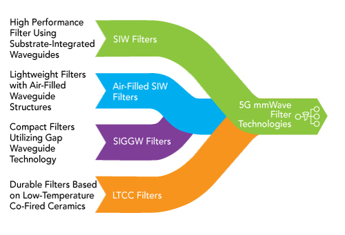
Figure 2 Various 5G mmWave filter technologies.
SIW Filters
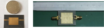
Figure 3 Cross-coupled SIW BPF10 and six-cavity SIW BPF.11
The substrate-integrated waveguide (SIW) is a technology that offers excellent performance at mmWave frequencies. It integrates the low loss characteristics of conventional waveguides with the compactness of a planar circuit. A cross-coupled SIW filter at 28 GHz with 600 MHz bandwidth and three transmission zeros was developed.10 The filter consists of an oversized cavity and a cascaded triplet. The oversized cavity provides a transmission zero (TZ) in the lower band due to the interaction of higher/lower order modes. In contrast, the cascaded triplet provides two TZs in the upper stopband. The in-band return loss is more than 15 dB, and the insertion loss is 2.7 dB. A SIW bandpass filter centered at 25.25 GHz was designed by J.-M. Huang et al., using six resonant cavities.11 Magnetic coupling was accomplished between the cavities by adjusting the opening between them. The filter exhibited a passband from 24.8 to 25.7 GHz with an insertion loss of 0.88 dB and return loss better than 12 dB. The fabricated prototypes of both filters are shown in Figure 3.
Air-Filled SIW Filters
This technology reduces the dielectric loss by utilizing an air-filled SIW (AFSIW) structure. This helps reduce the weight of the component while maintaining the performance, making it more suitable for aerospace and mobile applications. This variant reduces the insertion loss compared to the conventional dielectric-filled SIW techniques.
A fifth-order Chebyshev bandpass filter developed using AFSIW technology was developed by researchers.12 Iris inductive coupling topology was used to develop the filter based on the K-inverted model and Marcuvitz design flow. It has a fractional bandwidth (FBW) of 2.98 percent centered at 27.92 GHz and an insertion loss of 1.15 dB. For comparison, the researchers also evaluated a dielectric-filled SIW filter, which exhibited a higher insertion loss of 2.13 dB. An AFSIW filter was developed using non-resonant structures between the resonators. Although AFSIW technology is technically greater in terms of loss and bandwidth, researchers face challenges such as complex manufacturability and packaging difficulties.13
A cavity stacked contactless air-filled (CLAF) SIW BPF was developed.14 It supports multiple layers and has a robust assembly. It was a fourth-order filter with four stacked cavities utilizing irises for coupling. The iris layers were manufactured by metallizing the slot edges of a PCB, whereas the cavity layers were implemented using CLAF-SIW. The filter has a passband from 36 to 37.5 GHz. Figure 4a shows the filter assembly and the measurement setup and Figure 4b shows the response of the filter under test.
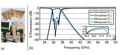
Figure 4 (a) Assembly and measurement setup (b) Filter response.
SIGGW Filters
A substrate-integrated gap groove waveguide (SIGGW) is an advanced planar waveguide technology. It features a perfect magnetic conductor formed by periodic vias and metallic patches on the top layer, a gap layer in the middle for wave propagation and a metallic bottom layer. It utilizes grooves and conductive posts to transmit EM waves through the air-filled gap, which rejects the need for solid dielectric material. As a result, it offers lower loss and a high Q factor.