
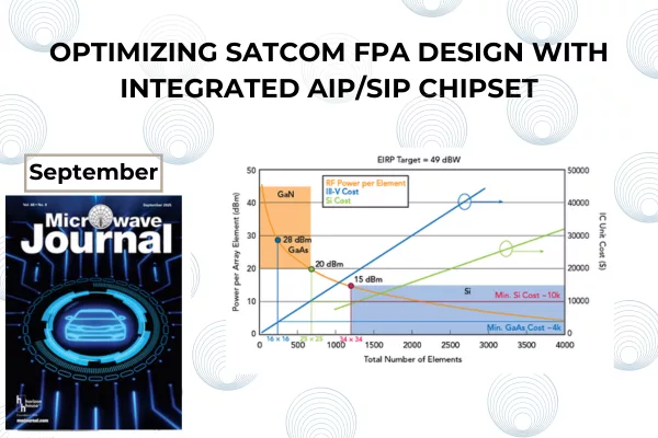
Figure 1 Conceptual diagram of 2 x 2 phased array antenna.
The rapid expansion of global satellite communication (satcom) systems,1 especially with the growing deployment of LEO satellite constellations, has created an urgent need for advancements in active antenna technology.2 Flat panel antennas (FPAs) are critical for delivering reliable, high speed connectivity and have been heavily investigated over the last few years.3 Current silicon-based designs for the phased antenna array face a radiated power per element bottleneck that causes upscaling of the array sizes to meet the transmit (Tx) link metrics. Circuits Integrated Hellas (CIH) has developed a groundbreaking approach to address these limitations by integrating III-V compound semiconductors with silicon technologies within a unified 3D package.4 Heterogeneous IC integration has attracted noticeable traction over the last few years,5 and CIH’s approach allows users to integrate components like power amplifiers (PAs), phase shifters and splitters within a unique, compact configuration. To date, no other commercial offering integrates III-V compound semiconductors and silicon ICs within a unified 3D system-in-package (SiP) and antenna-in-package (AiP) platform for FPAs. This article explores the technology and why it enables an unprecedented level of miniaturization, efficiency and cost-effectiveness.
PHASED ANTENNA ARRAY
In its simplest form, a phased antenna array for Tx operation is an antenna array where the individual elements are placed on a λ/2 grid, where λ represents the free space wavelength of the transmitted electromagnetic wave. An RF signal is equally distributed to each antenna branch, where its amplitude and phase are selectively manipulated by a typically silicon circuit with the collective term of beamformer IC, as shown in Figure 1. A 2 × 2 phased antenna array building block can be used to implement larger antenna arrays, depending on the transmission link needed for a specific satcom link.
CIH designs performant III-V components that fit the λ/2 array required in FPAs for ultra-high performance. This capability is at the core of the 3D heterogeneous integrations targeted in CIH’s development roadmap. The CIH solution involves integrating high performance compound semiconductors (III-V) such as GaAs and GaN with silicon substrates in a 3D configuration, creating a unified, compact SiP/AiP structure called the Kythrion™ platform.
WHAT IS KYTHRION?
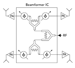
Kythrion is a family of highly integrated AiP beamforming modules designed to significantly enhance the performance and compactness of electronically steered arrays for space and ground-based satcom systems. Kythrion modules offer shared Tx/receive (Rx) apertures, multi-beam capability and ultra-fine control with 8-bit phase and gain resolution. With power-efficient analog front ends, on-chip telemetry and beam memory, Kythrion enables compact terminals with size, weight, power and cost (SWaP-C) metrics, achieving up to 36 dBm Tx output power and sub-1 dB receiver noise figures. These modules are tailored for next-generation FPAs for which performance per area, integration and fast beam agility are mission-critical. Figure 2 shows a conceptual architecture of the Kythrion 3D IC heterogeneous integration platform, where Figure 2a demonstrates the architecture for Tx/Rx satcom phased antenna arrays and Figure 2b shows a conceptual diagram of heterogeneous SiP integration.
Kythrion modules are intended for both transmit and receive operation, as shown in Figure 2, featuring an integrated dual-band antenna with switchable right-handed circular polarization (RHCP) and left-handed circular polarization (LHCP), supporting flexible link configurations across diverse orbital regimes. They include on-chip decoupling capacitors and electrostatic discharge (ESD) protection, are fully DC and RF tested at wafer level to ensure compliance with stringent electrical specifications and incorporate solutions for enhanced reliability and moisture ruggedness. Housed in low-temperature cofired ceramic (LTCC) packages with low thermal resistance, the modules enable PCB integration and reduced time-to-market, making them ideal for mission-critical satellite terminals and scalable RF front-end architectures.
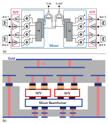
Figure 2 Conceptual diagram of a) Kythrion architecture and b) 3D IC SiP integration.
Figure 3 (a) Single antenna radiation pattern (b) 4 x 4 antenna array radiation pattern (c) S-parameters of a single antenna (d) top view of a 4 x 4 antenna array.
ENABLER 1: ANTENNA-IN-PACKAGE
AiP is a technology used to integrate an antenna directly into a semiconductor package, such as a system-on-chip (SoC), to save space and improve performance. This technology uses advanced packaging techniques to place the antenna near the RF circuitry. The antenna is typically designed to operate at a specific frequency band and has a certain polarization, depending on the application. Most commercial satcom take place in the Ku- or Ka-Band. The Ku-Band is usually selected for television broadcasting and data communication, whereas Ka-Band is used for high data rate communication links and broadband satellite services. Circularly polarized antennas are desirable in terms of polarization since they maintain communication between the transmitter and receiver, regardless of their relative orientation, and are excellent for mobility, weather penetration and reduction of multipath reflections.
CIH has developed a compact, single-aperture antenna element that integrates dual-band and dual polarization capabilities within a streamlined form factor. This advanced design supports simultaneous Tx and Rx operation, enabling full-duplex functionality and enhanced system efficiency. The element also provides circular polarization, making it well-suited for applications that demand robust performance in multipath and dynamic environments.
Building on this core technology, CIH has also engineered a Tx/Rx 4 × 4 antenna array based on the same dual-band, dual polarization element architecture as shown in Figure 3. Figure 3a shows the radiation pattern of a single Tx/Rx antenna array and Figure 3b shows the radiation pattern of a 4 x 4 antenna array. Figure 3c shows the S-parameters of a single Tx/Rx antenna and Figure 3d shows a top view of a 4 x 4 Tx/Rx antenna array. This scalable array solution offers integration density, improved beamforming flexibility and superior isolation between channels, making it ideal for next-generation communication systems, including 5G, satellite and advanced radar platforms.
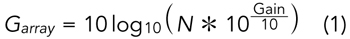
Figure 4 Tx antenna array sizing analysis.
ENABLER 2: HETEROGENEOUS INTEGRATION
For sizing an antenna array, as shown in Figure 4, CIH assumes a single patch antenna element has a gain of approximately 6 dBi, which is a typical value for microstrip patch antennas. Equation 1 shows the calculation for the theoretical gain of the antenna array Garray.
Where:
N is equivalent to the number of elements
G is equivalent to the gain of an element in dBi