

For example, when targeting an effective isotropic radiated power (EIRP) of 49 dBW, which is typical for a good uplink connection, we may formulate the total RF power (RFpower) needed from the antenna array using Equation 2.

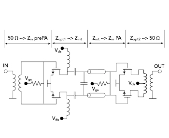
Figure 5 PA topology for III/V MMIC design.

Figure 6 Results for GaAs TSV RF transitions.
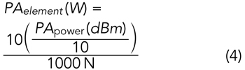
From the generated total RF power of the array, the power associated with the PA circuitry can be calculated using Equations 3, 4 and 5.


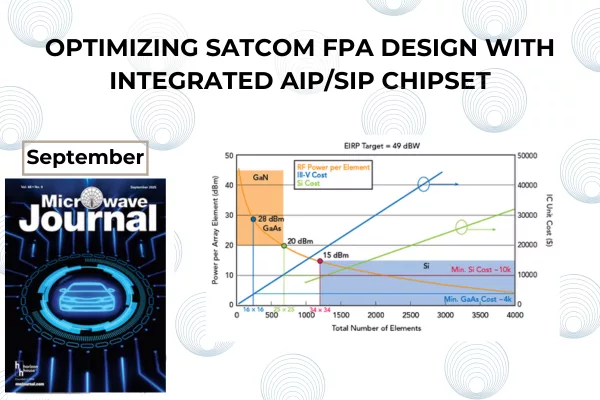
Following this chain of calculations, an antenna array size can be derived for each specific EIRP level required to maintain a good satcom link. An array size analysis graph is presented in Figure 4 for EIRP = 49 dBW, which is a typical Tx metric for a satcom uplink.
A traditional silicon-based array requires a 34 × 34 element configuration at 15 dBm per element, while an equivalent GaAs III-V enabled array achieves the same performance with just 25 × 25 elements at 20 dBm each, reducing the area by approximately 54 percent. Further optimization of the III-V parts reduces this area to 16 × 16 elements at 28 dBm, or about 22 percent of the silicon-based area, at a cost 40 percent lower than the silicon solution.
ENABLER 3: WAFER-LEVEL PACKAGE FOR III-V MMIC SIP
To achieve the integration levels required for FPAs, the CIH design approach departs from traditional compound III-V distributed components, favoring lumped passive components with improved back-end-of-line (BEOL) capabilities.
A differential unit amplifier, as described in Figure 5, was designed based on a mix between transformer-based and distributed passive component design that minimizes area with minor loss of performance. Additionally, through-silicon vias (TSVs) are employed to enable low loss, low-inductance RF routing off the chip.6
Figure 6 shows the wafer-level chip-scale package (WLCSP) experimental results for GaAs TSV RF transitions of an assembled test chip on a PCB. Further, the measured and simulated S-parameter response of a THRU line on the GaAs WLCSP test chip is presented. The entire chain, from PCB pad through the TSV and transmission line on the GaAs chip in a back-to-back configuration, is measured and found to exhibit 0.2 dB of insertion loss at 30 GHz. This low loss transition allows for compact MMIC design of RF circuits.
The design balances area optimization with performance retention, supported by TSV-enabled processes and air-bridge transitions. As can be seen from the de-embedded measurements, where the electrical reference plane is positioned directly below the TSV transition on the PCB level, the insertion loss of a THRU transition remains below 0.2 dB up to Ka-Band frequencies.
ENABLER – ARCHITECTURE EXAMPLE: IQ SWITCH FOR POLARITY CONTROL
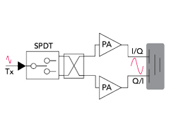
Figure 7 Tx unit module for polarization control.
One of the Kythrion variants, based on a Tx antenna element with dual polarization controlled by a dual-output amplifier switch module,7 allows for a Tx phased antenna array with controllable right-handed or left-hand circular polarization. The conceptual architecture is shown in Figure 7, where circuitry at the input of the amplifier is used to manipulate the I and Q components of the Tx signal. Depending on the configuration of the SPDT switch, the I and Q or Q and I signal constellations in the two PA branches are being amplified and fed to the Tx antenna resulting in either RHCP or LHCP.
Establishing RHCP or LHCP radiation at the antenna adds significant functionality to an antenna array based on such controllable RHCP/LHCP elements, since the uplink quality of the Tx antenna array can be controlled in real time for objects moving between satcom cells supporting either RHCP or LHCP radiation.
CONCLUSION
This work presents a pioneering approach to phased array antenna integration, achieved through the unique co-design and 3D packaging of III-V compound semiconductors with silicon technologies in a single SiP and AiP module. The engineering effort behind this platform has enabled experimental validation of key building blocks — demonstrating industry-leading miniaturization, low loss transitions and substantial reductions in array size and cost compared to conventional solutions. The architecture’s features are patent-pending.
While the technology is currently in the advanced prototype and experimental validation phase, the results underscore the transformative potential of this platform for next-generation satcom. These advances are the result of a multidisciplinary team and a sustained commitment to innovation in RF and packaging design.
References
- H. Al-Hraishawi, H. Chougrani, S. Kisseleff, E. Lagunas and S. Chatzinotas, “A Survey on Nongeostationary Satellite Systems: The Communication Perspective,” IEEE Communications Surveys & Tutorials, Vol. 25, No. 1, 2022, pp. 101–132.
- W. Hong et al., “The Role of Millimeter-wave Technologies in 5G/6G Wireless Communications,” IEEE J. Microwaves, Vol. 1, No. 1, 2021, pp. 101–122.
- X. Gu and D. Liu, B. Sadhu, “Packaging and Antenna Integration for Silicon-based Millimeter-wave Phased Arrays: 5G and Beyond,” IEEE Journal of Microwaves, Vol. 1, No. 1, 2021, pp. 123–134.
- E. Lourandakis, P. Fioravanti, G. Kontogiannopoulos and C. McMahon, “Heterogeneous AiP/SiP for Satcom,” International Conference on Compound Semiconductor Manufacturing Technology (CS MANTECH), May 19–22, 2025.
- W. Shi, C. Zou, Y. Cao and J. Liu, “The Progress and Trend of Heterogeneous Integration Silicon/III-V Semiconductor Optical Amplifiers,” Photonics, Vol. 10, No. 2, 2023, p. 161, MDPI.
- J.-C. Chiu et al., “An Ultracompact, Low-cost, and High-performance RF Package Technique for Wi-Fi FEM Applications,” IEEE Microwave and Wireless Components Letters, Vol. 30, No. 3, 2020, pp. 265–267.
- P. Fioravanti, E. Lourandakis, A. Gurulian and P. Bampali, “Single Pole Multiple Throw Power Amplifier Module,” European Patent Application, EP4489302A1.