

The development of antenna in package (AiP) modules for consumer applications, like 5G new radio (5G NR), has created several new challenges for the test and measurement industry, including high volume manufacturing (HVM) testing.
In the generic view of an AiP module shown in Figure 1, the 1 × 5 array of patch-like dual polarized radiators creates a beam in a direction perpendicular to the module antenna array plane. The AiP module may include a ball grid array or a board to flexible printed circuit connector on the backside for further assembly.

Figure 1 High-level diagram of an AiP module.

Figure 2 Example of a standard ATE test cell.
Testing a device under test (DUT) such as an AiP module in HVM requires over-the-air (OTA) measurements to test the antenna radiators and their feed structure, including the front-end parts of the transceiver electronic chips. This means that a measurement antenna must be integrated into the automated test equipment (ATE) test cell, which is a new requirement for commercial ATE test cells.1,2
Figure 2 shows an example of an ATE test cell comprising an Advantest V93000 ATE system able to test digital, power, RF and mmWave signals to a maximum frequency of 70 GHz, as well as an Advantest M4841 handler that automatically feeds packaged parts for testing.
Such test cells are the workhorse of the backend side of the semiconductor industry, where either finished silicon wafers or packaged devices need to be tested with high failure coverage and low cost-of-test (CoT). For example, they are used for conductive testing of mmWave devices at the wafer level.3 However, when the dies are integrated into an AiP module, mmWave conductive testing is no longer an option, and only OTA testing with a measurement antenna is possible.
In the high-level diagram of the manufacturing test flow for an AiP module (see Figure 3), a wafer containing the mmWave die that will be part of the AiP module is tested at the beginning of the flow. The testing can vary, for example, only DC parametric tests, mmWave loopback tests or even full parametric mmWave tests. The next step of the process is assembling the mmWave die into the AiP module. At this step of the process, techniques such as X-ray visualization can be used to check for failures in the assembly. Following the mmWave die integration, the AiP module, including the antenna array, can be tested. Again, at this stage, the test can be very basic (e.g., DC parametric and some built-in self-test) or it can include an OTA loopback test or full OTA parametric testing.

Figure 3 Example of a manufacturing test flow for an AiP module.

Table 1 lists typical tests performed at this stage in complete OTA parametric testing. Note that this test list differs from the one conducted in an anechoic chamber when characterizing the AiP antenna array or validating compliance testing with a specific standard. This test flow tests for good or bad devices and does not characterize the design. Finally, after the AiP module is tested, it is assembled as part of the final consumer device, such as a cell phone, and further testing is performed that may also include OTA testing of the complete final product.
From a CoT perspective, it is better to identify a bad DUT earlier in the manufacturing flow (shown in Figure 3), as it enables avoidance of expensive packaging, assembly or additional testing steps. Each AiP module manufacturer decides the exact test strategy and how much testing is done at each step.
HIGH VOLUME ATE OTA TEST OPTIONS
Production testing of mmWave components has traditionally been performed using bench equipment and rack-and-stack measurement setups with manual handling of the DUTs. This approach was feasible before the CoT pressure of consumer applications was present, but this changed with the usage of mmWave technologies in wireless consumer applications.
Achieving a low CoT with high failure coverage in HVM testing of AiP modules for 5G NR applications is not trivial. The semiconductor test industry has developed several strategies over the years to continuously reduce the CoT for consumer applications. One common technique is the use of multi-site testing. The challenge is how to apply these established strategies to HVM OTA testing.
Typical test strategies for HVM OTA testing are listed in Table 2. The most straightforward approach is to use a measurement antenna in the far-field region. This is very close to the typical setup used in anechoic chambers. However, in HVM OTA testing, the measurement antenna is fixed in a single position, which is usually perpendicular to the DUT antenna array. This approach has all the advantages of traditional antenna testing, but it presents several complex mechanical challenges for integration in a standard ATE test cell, especially for multi-site implementation. Single-site implementation in a commercial handler is feasible.1

The second approach addresses the mechanical challenge of integrating the OTA measurement setup into a standard ATE test cell by shrinking the physical distance between the AiP DUT and the measurement antenna, which can bring the measurement antenna into the radiating near-field region. This approach allows for a multi-site integration on a standard ATE test cell, which can result in a significant CoT improvement. However, there can be technical disadvantages associated with this approach, starting with the need to use a golden device calibration technique.
The final strategy is loopback testing. Loopback testing is a widespread approach for high speed digital and RF testing. It allows for a low-cost test approach since it does not require any mmWave measurement instrumentation. Usually, the objective is to be able to move to a loopback testing strategy once a product reaches a certain maturity level with the addition of some parametric OTA testing done on a sampling basis. The end user of the AiP module may expect a zero parts per million failure rate. However, OTA loopback testing can have several significant limitations,1 which makes its usage challenging.
Selecting the right strategy for OTA HVM production testing depends on various factors, for example, which stage the production ramp-up the device is in, experience with production testing of similar devices, etc. Because of this, the strategy may change depending on the stage of the DUT testing lifecycle.
Advantest has developed an HVM OTA test solution portfolio that can support the different test strategies described in Table 2 using commercially available ATE systems and standard handlers employed by outsourced semiconductor assembly and test companies. This is exemplified in Figure 4, which shows three different setups. Note that the DUT PCB test fixture is common to all three setups and contains eight DUT sockets that will allow parallel testing of eight AiP DUTs in production testing.
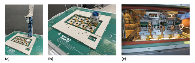
Figure 4 Different OTA test setups using the same DUT test fixture and program.
The setup shown in Figure 4a corresponds to a far-field measurement arrangement using an off-the-shelf dual polarized measurement antenna. The antenna opening is located 25 cm from the DUT antenna array. The measurement antenna is fixed perpendicular to the DUT antenna array. This setup is effective for performing OTA parametric measurements since it can be calibrated using standard antenna measurement techniques. This setup allows the test engineer to develop an initial test program and build the confidence needed on the ATE measurement instrumentation by validating a correlation with the bench reference measurement setup. This correlation only identifies good and bad devices and does not characterize the DUT or the antenna array design. This is why having a single position for the measurement antenna is acceptable for production testing.