

Heterogeneous integration promises a new era of high performance, mmWave integrated circuit (IC) technology that leverages diverse semiconductor materials from different foundries to realize a stable and distributed manufacturing ecosystem. While commercial markets have driven large-scale integration of RF silicon or silicon-on-insulator (SOI) CMOS processes, the underlying potential of these technologies to meet future requirements for satellite, wideband or defense systems is constrained to the physics of silicon.
Silicon technologies have become undifferentiated commodity solutions that support high volume manufacturing. PseudolithIC’s goal is to drive down the cost of compound semiconductor-based MMICs by an order of magnitude while harnessing CMOS RF, analog and digital circuits to complement the capability of compound semiconductors.
Compound semiconductor devices play a critical role in front-end RFICs, such as beamformers or transmit and receive (TRx) solutions, that support multiple functions using a single, shared set of electronic elements and/or antenna aperture-placing requirements. Achieving the best performance for different circuit blocks demands integration of CMOS with compound semiconductor components for front-end devices such as power amplifiers (PAs) and low noise amplifiers (LNAs). Beamforming arrays (BFAs) are an increasingly large commercial market, allowing for flexibility and efficient use of resources by integrating compact TRx ICs that support wideband operation with high efficiency and sensitivity.
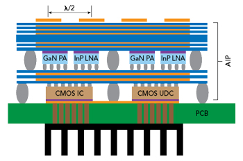
Figure 1 TRx front-end module.
Figure 1 shows a mmWave beamformer with a single antenna aperture that shares the TRx functions for communications and radar sensing. A single aperture with compact PAs and LNAs requires an antenna pitch of one-half the wavelength of the operating frequency, potentially on the order of millimeters at mmWave bands. This becomes a significant challenge above 30 GHz, leading to complicated packaging solutions such as the 3D packaging solution shown in Figure 1. The TRx front-end module in Figure 1 illustrates the 3D integration of a silicon CMOS beamforming RFIC, a compound semiconductor front-end MMIC and an antenna-in-package packaging concept.
MMICs based on compound semiconductors enable performance that exceeds standard CMOS. For example, applications with output power exceeding 20 dBm typically demand GaAs or GaN technologies. Table 1 shows an example of the available suite of device technologies that can be domestically sourced. It categorizes performance by output power, noise figure and switch performance measured as insertion loss.

Realizing a transmit (Tx)/receive (Rx) element with any of these materials increases the cost and complexity and creates a barrier to adoption. This barrier rises as more of these materials are assembled into a multi-chip module or an array of Tx/Rx elements.
PseudolithIC aims to lead commercialization toward rapid research and development cycles for new devices and has identified several vectors that benefit from this approach:
Area: The area of a MMIC is driven by the size of the matching and power supply bypass networks. Most of the area used to support a MMIC is dedicated to passive elements or power combiners, not the transistor. As technology moves into mmWave bands, the area of the MMIC makes using planar packaging solutions for BFA integration unrealistic. Consequently, 3D packaging is the solution, but this approach leads to higher costs. The PseudolithIC approach enables a die with larger dimensions to support a beamforming channel or array of channels.
Uniformity: The regular placement of compound semiconductor transistors across the wafer leads to improved device uniformity. As shown previously, compound semiconductors are typically fabricated on 4 or 6 in. wafers. Most of the chip area is occupied by inductors and transmission lines used in matching and bypass networks, rather than the transistors. Controlling these passive element values is more challenging in a compound semiconductor process than in silicon. Furthermore, the sparsity of the transistors may lead to doping variations across the wafer.
Yield: Due to the manufacturing uniformity, MMIC devices must be screened for known good die. Variations between the performance of different MMICs are significant, and devices are binned through screening. While yields in silicon are well over 99 percent, yields for compound semiconductor wafers are closer to 80 percent.
Cost: MMIC costs are determined by a combination of die area, wafer yield and the screening cost for known good die.
These factors suggest that MMICs will continue to struggle to satisfy the technoeconomic requirements of a high volume market for applications in microwave and mmWave bands, even as several large foundries are developing GaN-on-Si solutions. Despite the success of the GaAs HBT for PAs in handsets, the costs of other MMIC processes have pushed many commercial solutions toward Si or SiGe solutions. Additionally, the tool ecosystem has become incentivized toward processes that can use silicon fabrication processing tools.
The PseudolithIC approach is a heterogeneous integration process that uses compound semiconductor chiplets integrated into a silicon wafer to address these factors impacting compound semiconductor devices. CMOS plays an important role in the future success of compound semiconductors. It offers critical supporting roles in monitoring and controlling device operating conditions, device optimization for output power and efficiency, RF circuit blocks and analog circuits for linearization. The PseudolithIC platform aims to commercialize an X+CMOS process technology, where “X” is any combination of compound semiconductors. This platform enables any compound semiconductor technology to be combined with CMOS into a single die. It opens a new era in microwave and mmWave systems.
APPROACHES TO HETEROGENEOUS INTEGRATION
Alternative approaches for heterogeneous integration on RFICs have been considered through various advanced packaging and interconnect technologies. These approaches enable the combination of diverse functional blocks, such as high speed digital processors, RF front-ends and passive components, onto a single substrate or within a compact module. Common approaches include system-in-package, where multiple dice are co-packaged and connected; flip-chip bonding, which allows for high-density interconnects and reduced parasitics and through-silicon vias, used in 3D integration to vertically stack components for improved performance and reduced footprint.
Recent research and development efforts have focused on GaN-on-Si processes to support a more affordable platform for GaN device technologies. However, silicon substrates compromise the thermal path from the device to the package heat sink because silicon has worse thermal conductivity than silicon carbide. Moreover, GaN-on-Si processes are incompatible with CMOS device processing, limiting the ability to combine the advantages of analog and digital signal processing to improve device performance.
Advanced interposers, such as silicon or organic substrates, provide a platform for integrating different technologies with precise signal routing and thermal management. The PseudolithIC approach is categorized as an interposer-based approach where silicon CMOS is the preferred interposer. The compound semiconductor wafer is diced into chiplets, which are integrated into a single wafer through cavities etched into a silicon wafer. Interconnects are formed between the chiplet and the silicon interposer. Finally, the backside of the wafer can be metallized to create a thermal backplane that removes heat from the transistor through direct attachment to the silicon carbide or another substrate. PseudolithIC focuses on maintaining the best thermal solution for high efficiency and high-power devices while minimizing the interconnector parasitics between a compound semiconductor chiplet and the interposer. PseudolithIC products support a mix-and-match approach to choosing compound semiconductors. This approach creates competition among suppliers with different device technologies, enabling the OEM to configure the best technoeconomic performance.

Figure 2 Chiplet cost versus size.
PseudolithIC integration combines 8 or 12 in. commercial silicon CMOS wafers with compound semiconductors realized on 4 or 6 in. wafers. In any IC process, the cost of the die depends heavily on the size. Figure 2 shows the cost of a PseudolithIC chiplet versus the chiplet size, assuming 100 percent yield and a wafer cost of $20,000.
PseudolithIC’s approach does not demand scaling a compound semiconductor device to a larger wafer diameter. Depending on the transistor size, even a small wafer can provide tens of thousands of transistors. By constraining the wafer area to realize only transistor chiplets, the cost of each transistor drops dramatically relative to a MMIC. The $20,000 4 in. MMIC wafer will produce more than 20,000 450 × 450 µm chiplets, assuming 100 percent yield. The cost of each chiplet will be less than $1.00, driving down the cost of a heterogeneously IC solution. As the size of a chiplet approaches 100 x 100 µm, the chiplet cost drops below $0.20, in this example.
Packaging technology is becoming an important factor in meeting system requirements. This is especially true for the stringent performance, size and power requirements of 5G, radar and wireless communications applications. The packaging approach is also crucial for maintaining a sustainable cost structure.
RAPID PROTOTYPING AND IP BLOCK DEVELOPMENT
The PseudolithIC integration approach enables rapid prototyping with devices at different technology readiness levels. PseudolithIC has demonstrated nascent N-polar Ka-Band GaN MMICs, developed through the support of the Office of Naval Research. Using an 80 nm GaN HEMT process technology, a 6 in. N-polar SiC wafer was dedicated solely to transistor chiplets. In contrast, the silicon interposer could be used to experiment with variations of matching networks to determine, with rough models, the best experimental matching network for the device. This device experimentation model helps to support rapid “lab-to-fab” capability and the insertion of device technologies into beamforming systems.
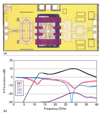
Figure 3 (a) 90 nm GaN Ka-Band amplifier. (b) S-parameters of two GaN amplifiers.
More recently, PseudolithIC has continued to advance the rapid lab-to-fab concept as part of the CHIPS Act. Led by the University of Southern California Information Sciences Institute, the Defense Ready Electronics and Microdevices Superhub, CA DREAMS is one of eight regional innovation hubs established under the Department of Defense Microelectronics Commons Program. This strategic initiative is funded by the CHIPS and Sciences Act of 2022 to develop onshore microelectronics hardware prototyping.
Here, a few highlights from Pseudolithic’s rapid prototyping capability are illustrated. The first two examples are based on a 90 nm GaN HEMT technology while the latter two highlight results in using commercial InP HBT and GaN HEMT technologies. PseudolithIC highlights other Ka-Band components that might be integrated into a BFA, including an InP HBT PA that offers excellent gain compression, high efficiency and a high gain 2-stage GaN PA.
Ka-Band 2 W GaN PA
As part of the CA DREAMS Hub, a single-stage Ka-Band PA was designed with the pre-commercial 90 nm GaN HEMT process. The die layout is shown in Figure 3a, and measurements on two devices are shown in Figure 3b. These devices achieve a peak gain of 11 dB at 28 GHz. Preliminary large signal measurements could not compress the PA but show linear PA performance to 30 dBm with greater than 25 percent PAE.
Ka-Band 4 W GaN Switch
TRx front-ends require an SPDT switch to control the signal flow from a common antenna node, such as a device antenna, to the TRx paths. A suitable switch technology for the power levels required in commercial and defense beamformers combines high RF power handling, low on-resistance and low off-capacitance. One approach to meet the SPDT requirements is the customization of wide-bandgap devices. Figure 4a shows the switch realized with the same pre-released 90 nm GaN HEMT technology with a HEMT optimized for a switch chip integrated into a standard silicon interposer wafer using the PseudolithIC process and Figure 4b shows insertion loss and isolation measurements for multiple devices.

Figure 4 (a) Single stage 90 nm Ka-Band GaN RF switch. (b) 90 nm, Ka-Band GaN RF switch insertion loss and isolation.