


The switch FETs are integrated into a shunt configuration with a quarter-wave line routed back to the common port. Other device technologies, such as SOI switches, offer tremendous capability when coupled with GaN devices to realize unique heterogeneous structures.
Ka-Band 100 mW InP HBT PA
While GaN PAs have received substantial attention for high-power applications, they might not be ideal for pre-driver applications requiring high linearity and efficiency. When working with a single device technology, designers are often limited to pre-driver amplifiers with high DC power consumption to achieve outputs close to 20 dBm. At this output power range, many other device technologies, such as InP HBTs, have become great candidates for the high efficiency pre-driver function. Figure 5a shows a single-stage 250 nm InP HBT implemented in the PseudolithIC process. Figure 5b shows the large signal characterization results of three samples measured at 28 GHz. Saturated output power is 20.5 dBm with an output P1dB of 20 dBm and 35 percent peak PAE. This demonstrates the ability of the PseudolithIC platform to use various device technologies in the same silicon platform.
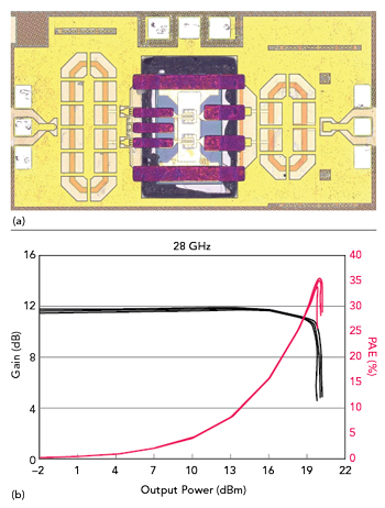
Figure 5 (a) Single-stage Ka-Band InP HBT PA. (b) Ka-Band InP HBT PA performance.
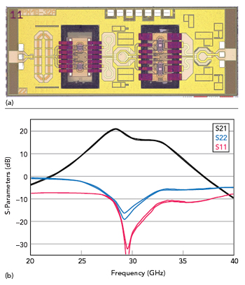
Figure 6 (a) Two-stage Ka-Band GaN HEMT PA. (b) Performance of two-stage GaN HEMT PA.
Two-stage Ka-Band GaN PA
Figure 6a shows the micrograph for a two-stage 150 nm GaN HEMT amplifier. The gain of the PA is more than 21 dB at 28 GHz and the amplifier operates from 26 to 32 GHz. The micrograph of the PA shows several different metal layers that create matching networks that would not have been possible in a typical compound semiconductor process. Figure 6b shows the small-signal characterization of the amplifier.
CMOS EMPOWERS COMPOUND SEMICONDUCTOR DEVICES
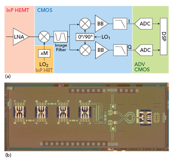
Figure 7 (a) Opportunities for heterogeneous integration in an mmWave receiver. (b) Micrograph of mmWave receiver.
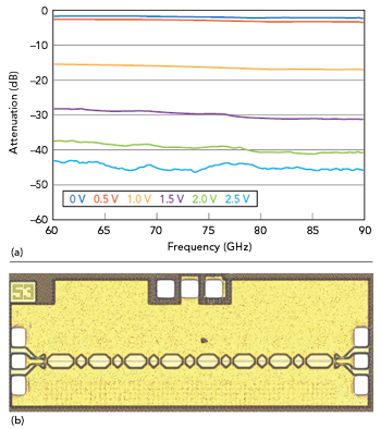
Figure 8 W-Band CMOS attenuator covering E-Band (60-90 GHz) with more than 40 dB of attenuation.
PseudolithIC has demonstrated a variety of semiconductor devices integrated into a silicon interposer. The IP blocks can be used to construct unique front-end IC solutions that support large-scale beamformers or other highly-integrated microwave systems. The advantage of the PseudolithIC approach is that each block can be customized for customer requirements. As shown in Table 1, the device technology that best supports the customer’s technoeconomic requirements is used to support the development of a Tx/Rx front-end.
PseudolithIC is developing solutions incorporating CMOS digital, analog and RF circuitry to support compound semiconductors in manufacturing, test and operation to address these limitations. The advantages of CMOS are severalfold:
Built-in self-test: By building self-test with analog signals or digital scan chains, users can rapidly assess the health of a heterogeneously integrated solution without an extended test period.
Analog bias and power management: CMOS process nodes can support biasing circuits that compensate for device variations locally instead of resorting to external monitoring and trim. The threshold voltage of a compound semiconductor device compensates for larger device-to-device variations and circuit yield considerations.
RF signal blocks: Mature CMOS processes can be used for applications up to 90 GHz by developing CMOS blocks such as mixers, phase shifters, attenuators, variable gain amplifiers and frequency multipliers.
Signal processing: An advantage of CMOS is the ability to incorporate digital signal processing. Different functions can be incorporated into the solution by using different CMOS IP blocks, possibly as chiplets.
PseudolithIC’s X+CMOS products enable customization of front-end IC solutions for different microwave and mmWave frequency bands. Furthermore, the compatibility of the PseudolithIC solution with standard silicon packaging approaches aids integration into customer solutions. Figure 7a shows the potential for implementing InP and CMOS technologies in an mmWave receiver via a block diagram and Figure 7b shows the corresponding micrograph.
E-BAND INTEGRATION OF MULTIPLE TECHNOLOGIES
PseudolithIC has developed a CMOS-enabled W-Band InP HEMT LNA. This design can be integrated into higher functionality systems like a heterodyne receiver. A variety of different technologies can be used as building blocks for the receiver. These might include InP HEMT for the LNA, InP HBT for the frequency doubler, RF CMOS for the receiver blocks and an advanced node for the ADC and other signal processing features. Mixing technologies enables the building blocks to optimize the receiver’s performance.
To provide gain control for the InP HEMT LNAs, CMOS attenuators have been designed in the PseudolithIC integration process. Gain control ensures the proper signal strength and prevents receiver compression. Using the PseudolithIC integration process results in a more compact solution than standalone GaAs-based attenuators can provide. Figure 8 shows measurements of an 8-stage W-Band attenuator integrated into an X+CMOS solution.
The device has been measured in E-Band, from 60 to 90 GHz, with a control range of 0 to 2.5 V in 0.5 V steps. This design achieves an insertion loss of 1.6 to 2.3 dB with a maximum attenuation value of at least 42 dB over the entire frequency range. The return loss is better than 10 dB under all attenuator states, and the solution has a power compression level of more than 10 dBm. This performance is comparable to GaAs technologies, but at a lower cost. As the industry seeks more sophisticated solutions, the flexibility to add lower cost CMOS IP blocks such as this attenuator becomes a significant advantage of a PseudolithIC solution.
PSEUDOLITHIC PRODUCT ROADMAP
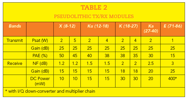
PseudolithIC is developing TRx modules and other highly-integrated RFIC blocks from X- to E-Band frequencies. A summary of the capabilities of these early release parts is illustrated in Table 2.
Acknowledgment
The authors acknowledge the support of NSTXL through a Microelectronics Commons Subcontract under the CA DREAMS HUB as well as SBIR support through the NSF (Dr. Elizabeth Mirowski), DARPA (Drs. D. Meyer, D. Abe, T. Kazior, and T. Hancock), AFRL (Dr. A Mattamana), DOE (Dr. P Sayer) to undertake the work described in this publication. A portion of this work was performed in the UCSB Nanofabrication Facility, an open access laboratory. The authors acknowledge the use of the Quantum Structures Facility within the California Nanosystems Institute, supported by the University of California, Santa Barbara and the University of California, Office of the President. The US Government has cleared the publication for release titled “Heterogeneous Integration Brings Compound Semiconductors into the Age of RF CMOS” (Distribution Statement A: Approved for public release. Distribution is unlimited).